HiSiliconhi3519dv500Development Board-EMMCVersion
Project: Board Introduction | page_id: 1057
| HI3519DV500 Development Board | |
|---|---|
| Board Function Type | XSTRIVE- |
| CPU | hi3519dv500 |
| Video Encoding | Supports H.265/H.264 encoding/decoding |
| Maximum resolution 3840x2160@30fps” | |
| Video Input | 3840x2160@30fp |
| Audio Input | Sampling rate: 8K/12K/16K/24K/32K/44.1K/48K |
| Audio Output | Supported |
| USB | 1 x USB2.0 |
| Network | RJ45 10/100M |
| Operating Temperature | 0 to 70°C |
| Service Life | Continuous operation life of more than 2 years |
| DDR | 8Gbit*2 = 2GB |
| EMMC | Supports eMMC5.1 16G |
| Number of Ethernet Ports | 1 |
| Number of Sensors | 1 |
| Computing Power | 2.5TOPS INT8, can be used for face recognition, electric bicycle recognition, pedestrian recognition, etc. |
1. Product Images
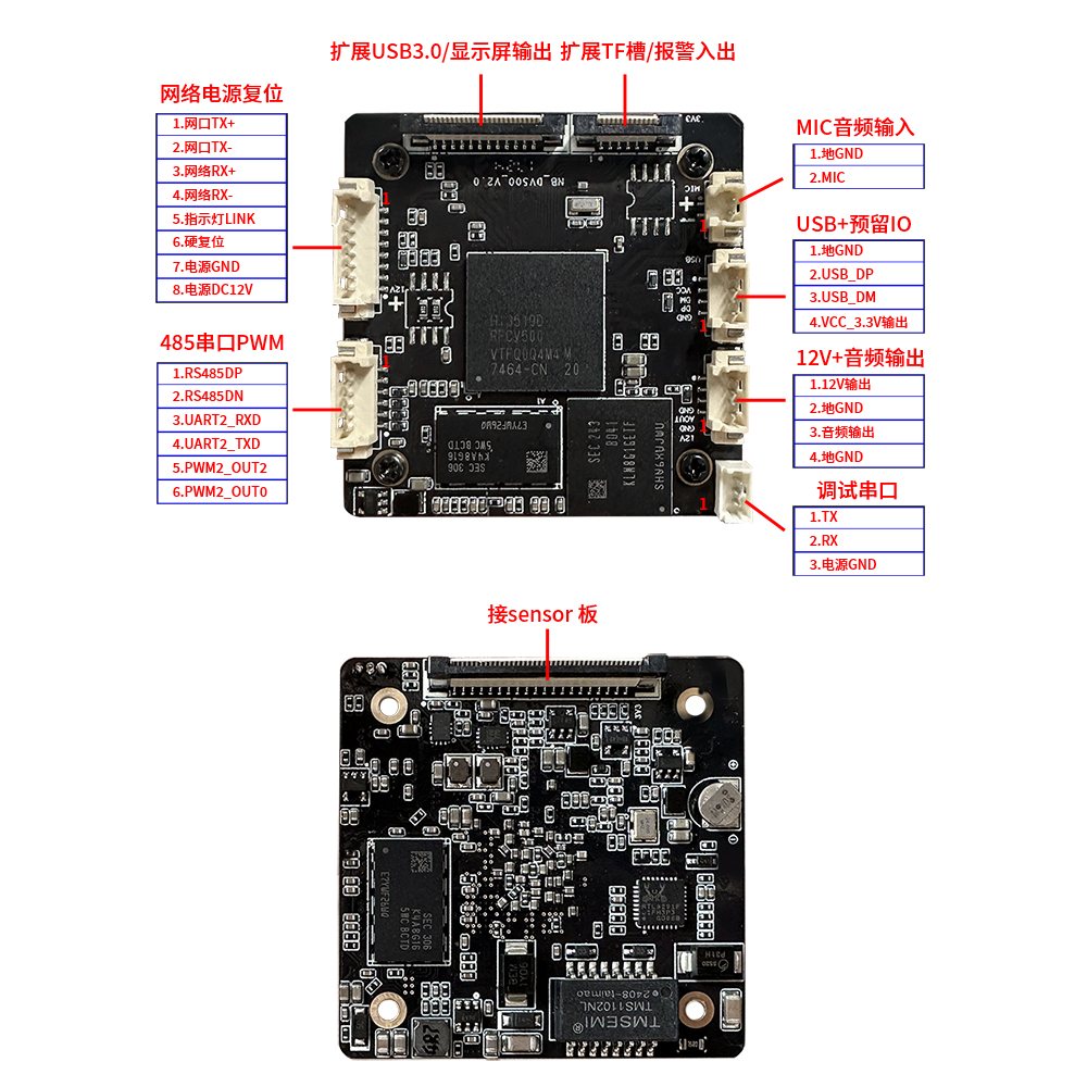
Board dimensions 45*45mm
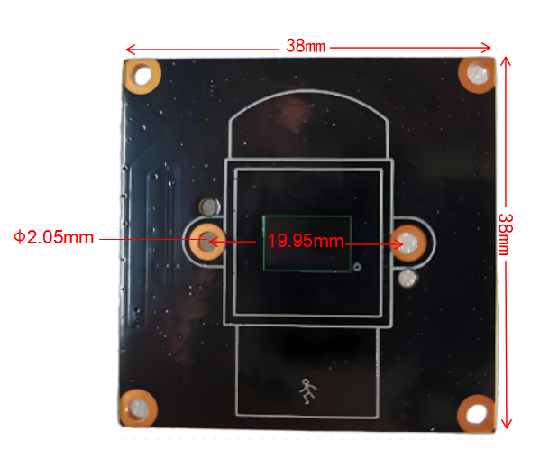
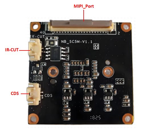
①SC450AI Sensor Board (silkscreen NB_SC5M-V1.1)
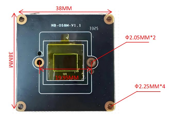
②OS08A20 Sensor Board (silkscreen NB_OS8M-V1.1)
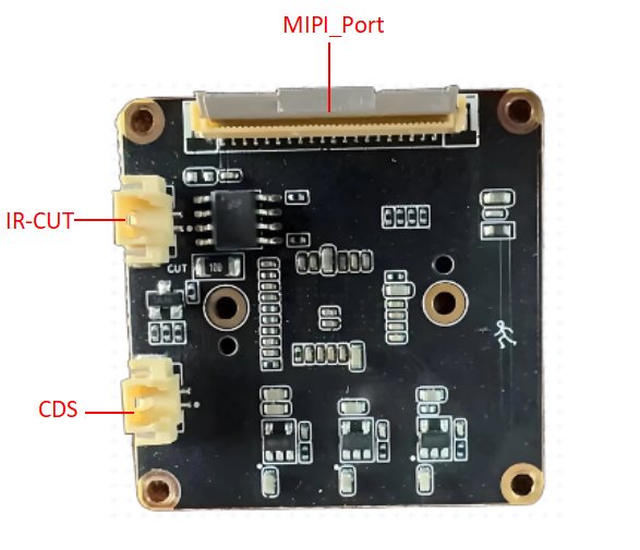
2. Core Board Function Interface Description:
(1) Main board single-channel sensor iic3
4lane mipi (default); with a custom sensor adapter board it can also support dual-channel sensor
2lane mipi;
(2) USB2.0 is not a power input; the default is DC3.3V output, for expanding the WIFI wireless function board;
(3) SMD RTC for local time synchronization;
(4) Function expansion 1 uses a 12pin FPC connector to expand TF storage, WIFI, alarm input/output, and speaker amplifier output;
(5) Function expansion 2 uses a 24pin FPC connector to expand USB3.0, BT656, and display output interface;
(6) A sop08 packaged i2c encryption position is reserved.
3. Core Board Function Interface Definition:
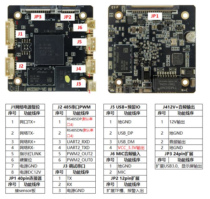
4. Interface Circuit Diagrams
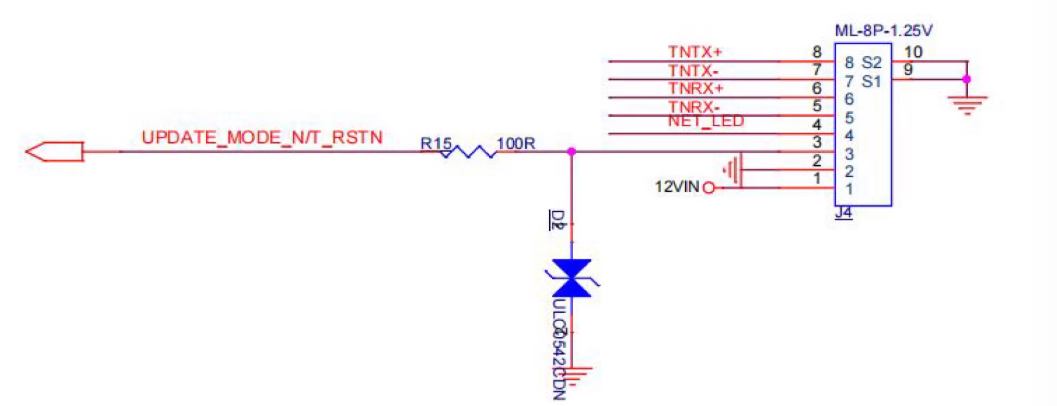
1、8PIN 100M Ethernet port, reset update burning and 12V power interface J4; Reset IO: GPIO0_0
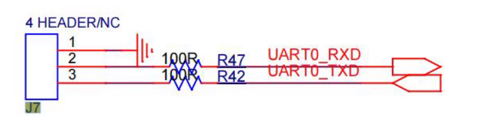
2、3PIN UART0 debug serial port J7
3、USB2.0 socket, default 3.3V power output J11
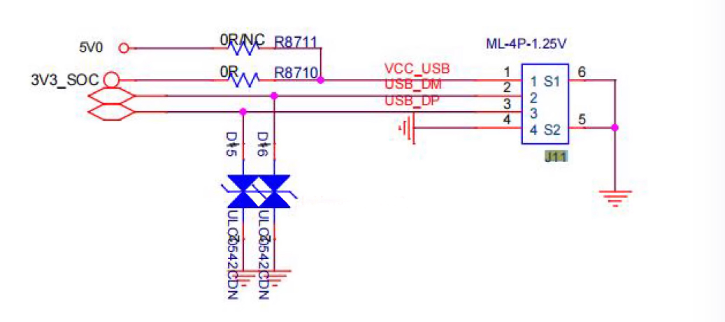
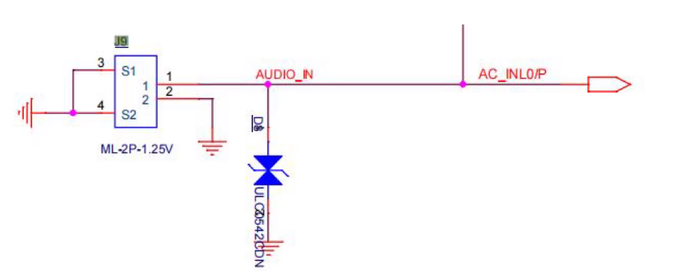
4、Audio input J9, audio output and DC12V output J1
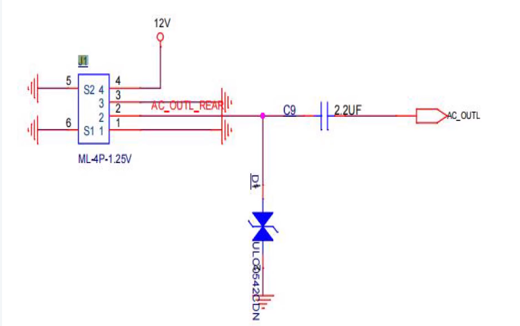
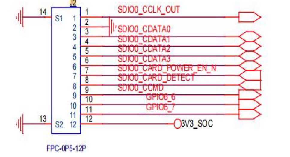
5、12PIN 0.5mm socket for SD card and alarm interface Alarm input: GPIO6_6 Alarm output: GPIO6_6
6、40PIN 0.5mm socket for sensor interface
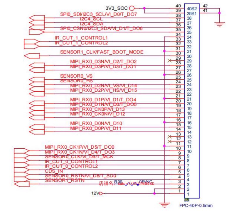
The interface supports 4-lane MIPI single sensor and is compatible with sensor boards with MIPI interface
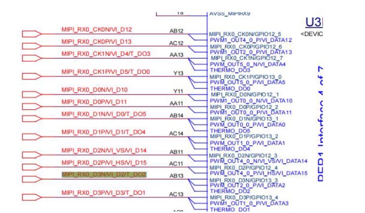
CPU MIPI interface:
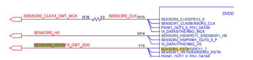
I2C address: I2C3, sensor clock and reset signal:
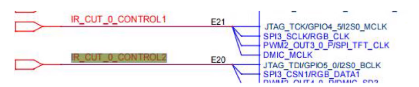
PIN6 and 7: IRCUT control output signals: GPIO4_5 and GPIO5_0
PIN5: color-to-black input signal, reserved GPIO: GPIO1110_2

7、RTC and encryption IC interface
RTC synchronization uses the internal RTC clock of HiSilicon;
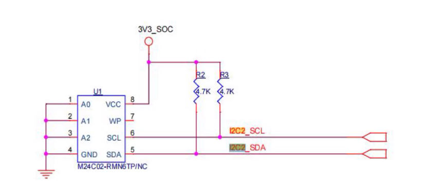
An encryption IC position is reserved on the board; the encryption ICs all use the I2C interface; the corresponding CPU interface is I2C2
8、PWM port and 2 serial port groups J6
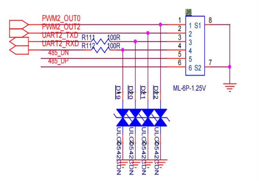
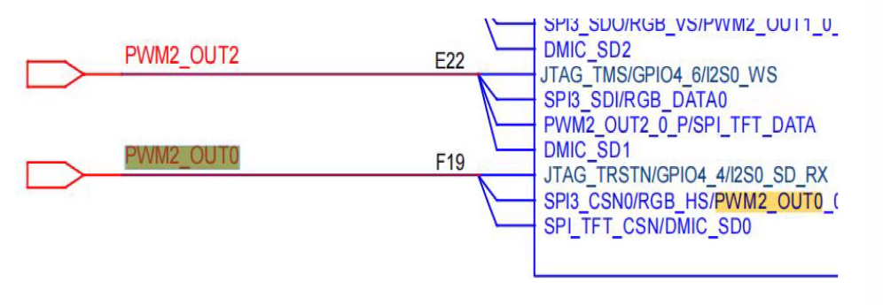
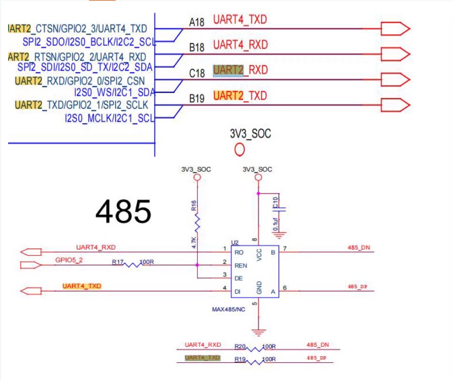
2 serial port groups: UART2 and UART4 by default; adding an RS485 IC can change the UART4 serial port to an RS485 port
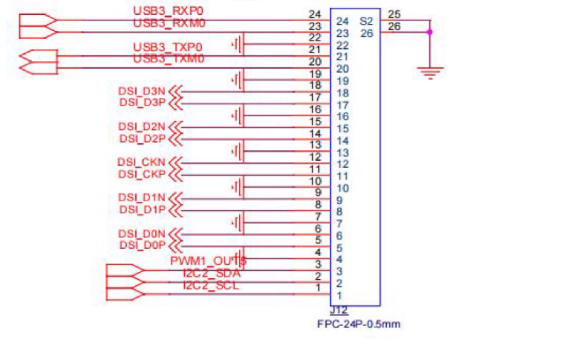
9、24PIN 0.5mm socket for USB3.0 output, DSI display interface, PWM port and multiplexed I2C2 interface

5. Core Board Configuration and Supported CMOS and Expansion Function Description
4.1、Default hardware configuration of the HiSilicon core board
2GB DDR +8G EMMC (the DDR and EMMC capacity can be changed for mass production)
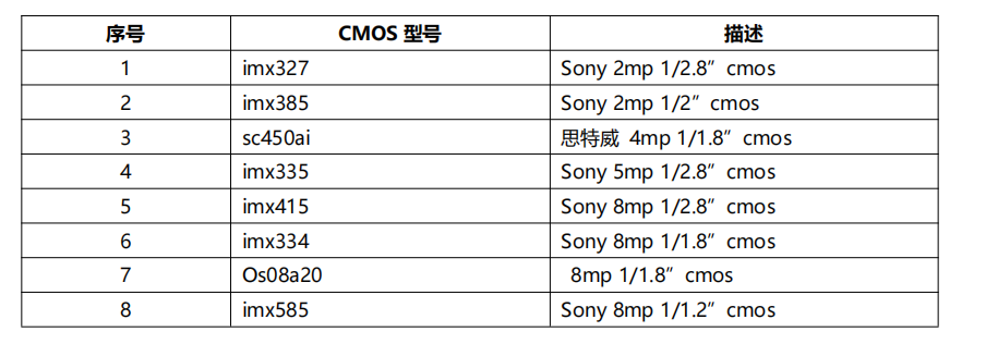
4.2、Supported CMOS boards:
4.3、Supported function expansion boards:
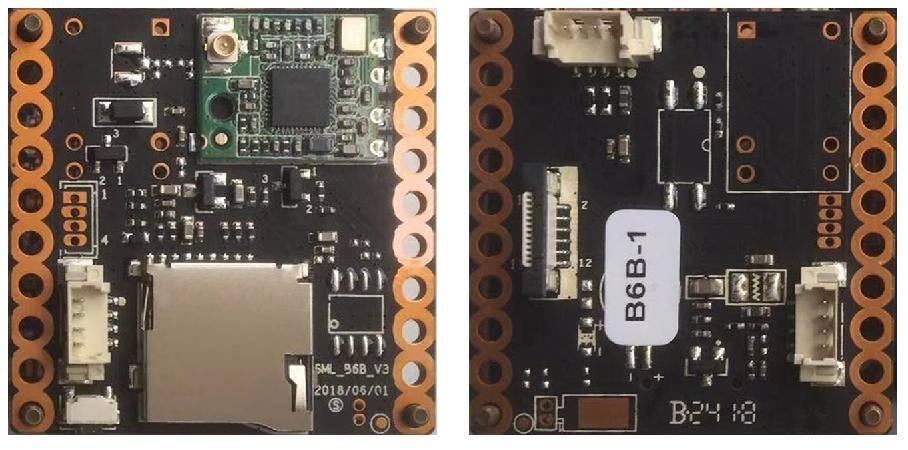
Expandable functions: 1. TF card slot 2. Switch value alarm input/output 3. WIFI wireless
6. FAQ
| Question | Answer |
|---|---|
| 1、 | |
| 2、 | |
| 3、 | |
| 4、 |