KM01A-ZD3336 AOV Board Specification
1 Overview
1.1 What is AOV
AOV (Always On Video) is the mainstream technology route for solar-powered low-power cameras. Unlike a conventional PIR-triggered camera (“PIR senses a person → wakes the SoC → starts recording”), AOV instead keeps the video path always on at low power, runs scene analysis locally on the on-board NPU, and only raises the recording profile and wakes the wireless uplink once a valid target has been confirmed.
| Dimension | PIR-triggered | AOV (this board) |
|---|---|---|
| Dimension | PIR-triggered | AOV (this board) |
| Trigger source | Difference in infrared heat radiation | On-image AI analysis (person / vehicle / abnormal sound) |
| Detection coverage | Within the PIR cone | Full frame field of view |
| Slow movement | Often missed | Detectable (as long as it is in frame) |
| Pre-event context | Often cut off by wake-up latency | The pre-roll buffer is already recording |
| Recording continuity | Event clips, discontinuous | Continuous low bitrate + stitched HD event clips |
| Power profile | Saves power through deep sleep | Saves power through “low-power always-on + on-demand upgrade” |
The cost has to be stated clearly: AOV draws more continuous power than a PIR wake-up design, so it places higher demands on solar panel wattage, battery capacity and charge/discharge management — which is exactly why the power path, RTC wake source and TF card write policy of an AOV board are the core of any product design.
1.2 Where this board sits in an AOV product
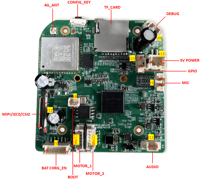
The KM01A-ZD3336 is the main control board of an AOV 4G PTZ camera: it carries all computing, networking, storage and PTZ control, and interfaces with the rest of the product through MIPI / pin headers, the TF socket, motor connectors, the battery connector, the 4G antenna connector and the mechanical parts.
Low-power always-on + event upgrade: the built-in NPU of the KM01 analyses the scene locally, so the full video stream never has to go to the cloud;
Day/night switching loop: IR-cut filter switching + white-light fill PWM + infrared fill light, all scheduled by the SoC;
Solar power loop: battery charge/discharge interface + charge enable + resistive-divider battery sampling (AIN0), working with an external solar panel and charge IC;
Cable-free networking: a 4G Cat.1 bis module is soldered straight onto the board and event clips are sent back over LTE;
Local storage: the TF socket takes large-capacity high-endurance cards for continuous writing;
PTZ control: dual H-bridges drive the horizontal / vertical DC motors directly, with no external driver board.
1.3 Key specifications at a glance
| Dimension | Parameter |
|---|---|
| Product form | AOV low-power 4G PTZ camera mainboard (common base board for bullet and dome cameras) |
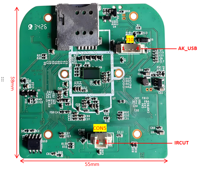
| Board size | 58 mm × 55 mm |
| Main controller | ANYKA KM01 series (board silkscreen D611, QFN88) |
| CPU core | ARM926EJ-S single-core RISC, up to 900 MHz |
| On-board memory | 512 Mibit / 1 Gibit DDR2 SDRAM |
| AI unit | NPU: object detection/tracking, face detection/recognition and other algorithms |
| Video encoding | H.265/H.264 hardware encode up to 3072×2048; JPEG up to 16384×8192 |
| Camera input | Three MIPI CSI differential pairs + DVP, two CIS inputs supported |
| Connectivity | 4G LTE Cat.1 bis (ML120H module soldered on board) + Ethernet MAC |
| Storage | TF socket (Micro SD, high-endurance card) + 128 Mbit SPI flash on board |
| Power | 5 V DC input + Li-ion battery (BAT+), solar panel charging supported (CHRG_EN) |
| Battery level sensing | BAT+ dual 100K divider → AIN0 |
| PTZ | Dual H-bridges driving the horizontal / vertical DC motors directly |
| Fill light and filtering | IR-cut filter switching, white-light PWM dimming, infrared fill light, LED status indication |
| Audio | Differential MIC input + Class-D speaker output |
| Wake source | PIR (IR), remote 4G command, TF card insertion (TF_DET), reset button |
| Operating temperature | To be confirmed (not specified by the vendor; -20 °C to +60 °C suggested for outdoor use) |
2 AOV operating modes and power state machine
This is where an AOV board differs most from an ordinary IPC board. The product firmware schedules the state machine below, and on the hardware side each state switches a different set of modules on this board on or off.
| State | Video path | AI inference | 4G module | Fill light | Motor | Note |
|---|---|---|---|---|---|---|
| State | Video path | AI inference | 4G module | Fill light | Motor | Note |
| Deep sleep | Off | Off | Power off / PSM | Off | Disabled | The only entry point for PIR or timed wake-up, and the lowest power target |
| Always-on standby | Continuous recording at low resolution and low frame rate | Always-on detection | Stays registered on the network but with low activity | Off | Held | The core AOV state; the pre-roll buffer is produced here |
| Event confirmation | Raised to the target resolution / frame rate | Compute raised | Wake up, prepare upload | White light / infrared triggered | Rotates on demand | Entered once AI decides the target is a valid one such as a person or a vehicle |
| Event recording | Full-quality recording + pre-roll stitching | Continuous tracking | Transmitting clips | Held until the event ends | Returns on demand | Writes to the TF card and uploads |
| Remote live preview | High-quality streaming | On demand | Sustained high-speed uplink | Optionally enabled | PTZ tracking | Started by the user; the highest power state and not meant to stay on |
| Night mode | Always on or event triggered | Same as above | Same as above | Infrared fill light + IR-cut filter switching | Same as above | Switched by the light sensor or an RTC schedule |
Three hardware constraints behind this state machine(mandatory for any product design):
1. Wake-up must be interruptible by a hard-wired PIR line. IR (GPIO68) on J15 is that path: the PIR output pulls the GPIO directly to wake the SoC from deep sleep, with no dependency on the 4G module being online.
2. The 4G module and the main controller must save power independently. The ML120H supports power-off (55 uA), sleep (0.41 mA) and standby (5.64 mA); only together with the SoC sleep policy does AOV battery life become possible.
3. TF card writing is a continuous load. Continuous AOV writing requires a high-endurance (surveillance-grade) card; ordinary cards wear out quickly under constant writing.
3 Board basics
| Item | Parameter |
|---|---|
| Product form | AOV low-power 4G PTZ camera mainboard (common base board for bullet and dome cameras) |
| Board size | 58 mm × 55 mm |
| Main controller | ANYKA KM01 series (board silkscreen D611, QFN88) |
| CPU core | ARM926EJ-S single-core RISC, up to 900 MHz |
| On-board memory | 512 Mibit / 1 Gibit DDR2 SDRAM |
| AI unit | NPU: object detection/tracking, face detection/recognition and other algorithms |
| Video encoding | H.265/H.264 hardware encode up to 3072×2048; JPEG up to 16384×8192 |
| Camera input | Three MIPI CSI differential pairs + DVP, two CIS inputs supported |
| Connectivity | 4G LTE Cat.1 bis (ML120H module soldered on board) + Ethernet MAC |
| Storage | TF socket (Micro SD, high-endurance card) + 128 Mbit SPI flash on board |
| Power | 5 V DC input + Li-ion battery (BAT+), solar panel charging supported (CHRG_EN) |
| Battery level sensing | BAT+ dual 100K divider → AIN0 |
| PTZ | Dual H-bridges driving the horizontal / vertical DC motors directly |
| Fill light and filtering | IR-cut filter switching, white-light PWM dimming, infrared fill light, LED status indication |
| Audio | Differential MIC input + Class-D speaker output |
| Wake source | PIR (IR), remote 4G command, TF card insertion (TF_DET), reset button |
| Operating temperature | To be confirmed (not specified by the vendor; -20 °C to +60 °C suggested for outdoor use) |
4 Interface definition
4.1 Interface overview
| Designator | Interface | Type | Role in an AOV product |
|---|---|---|---|
| J13 | 5V POWER | 2P / 2.00mm | 5 V DC input (adapter, or solar panel through a charge IC) |
| J9 | DEBUG | 3P / 1.25mm | UART0 debug port |
| J15 | GPIO | 2P / 1.25mm | PIN1 = IR (PIR wake input), PIN2 = WL (white-light fill control) |
| J1 | MIC | 2P / 1.25mm | Analog microphone differential input (abnormal sound detection / voice) |
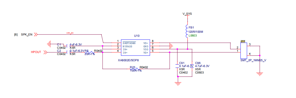
| J11 | AUDIO | 2P / 1.25mm | Speaker output (two-way talk / audible and visual alarm) |
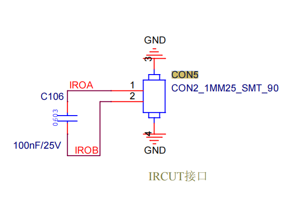
| CON5 | IRCUT | 2P / 1.25mm | IR-cut filter switching (day/night switching) |
| J8 | BOOT | 2P | BOOT shorting header (in production make sure the jumper is not fitted) |
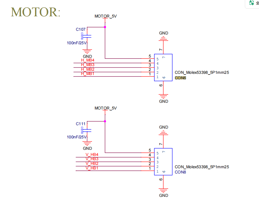
| CON6 | MOTOR_1 | 5P / Molex 53398 | Horizontal PTZ motor H-bridge output |
| CON8 | MOTOR_2 | 5P / Molex 53398 | Vertical PTZ motor H-bridge output |
| J5 | BAT CHRG_EN | 5P | Battery connection + charge enable + battery level sensing |
| J10 | AK_USB | 4P | USB 2.0 + 5 V supply (production test / upgrade) |
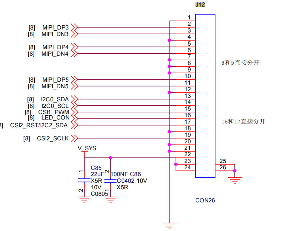
| J12 | MIPI/I2C0/CSI2 | 26P | Image sensor input + fill-light PWM + indicator LED + 5 V |
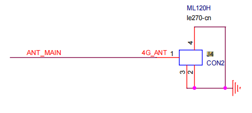
| J4 | 4G_ANT | IPEX | 4G module RF antenna interface |
| J3 | TF Card | TF card socket | Local recording storage (high-endurance card recommended) |
4.2 How the key AOV interfaces are split
The main functional blocks of an AOV product map onto this board as follows:
| AOV requirement | Where it lands on this board | Interface / signal |
|---|---|---|
| AOV requirement | Where it lands on this board | Interface / signal |
| Hard-wired PIR wake-up | J15 PIN1 | GPIO68 (IR) |
| White-light fill on/off | J15 PIN2 | GPIO67 (WL) |
| Fill-light brightness adjustment | J12 PIN15 | CSI1_PWM (PWM dimming) |
| Day/night switching (filter change) | CON5 | IROA / IROB |
| Status indicator | J12 PIN16 | LED_CON |
| Main / secondary image sensor | J12 | Three MIPI_DP/DN 3/4/5 differential pairs + I2C0_SDA/SCL |
| Sensor reset | J12 PIN17/19 | CSI2_RST, CSI2_SCLK |
| Local recording | J3 | TF card socket (TF_DET detects insertion/removal) |
| Solar / battery input | J13 / J5 | VCC_5V / VBUS / BAT+ |
| Charge enable | J5 PIN4 | CHRG_EN |
| Battery level sampling | J5 PIN5 → AIN0 | R29 / R33 divider |
| 4G data upload | J4 + module | ANT_MAIN; the module talks to the SoC over USB/UART |
| PTZ horizontal / vertical | CON6 / CON8 | H_MB1~4 / V_HB1~4 |
| Event audio reference | J1 | MIC_P / MIC_N |
| Alarm sound | J11 | VO+ / VO- |
4.3 Pin definition details
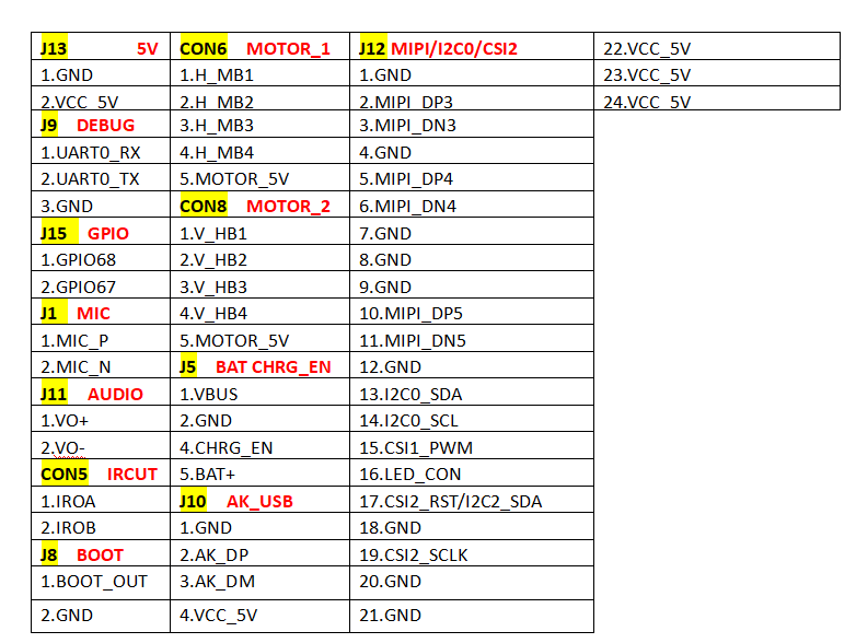
J13 5V POWER (2P / 2.00mm)
| Pin | Signal | Note |
|---|---|---|
| 1 | GND | Ground |
| 2 | VCC_5V | 5 V DC power input (solar panel through a charge IC, or an adapter directly) |
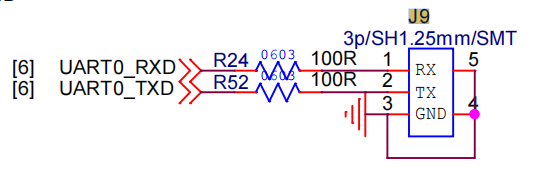
J9 DEBUG (3P / 1.25mm)
| Pin | Signal | Note |
|---|---|---|
| 1 | UART0_RX | Debug UART RX |
| 2 | UART0_TX | Debug UART TX |
| 3 | GND | Ground |
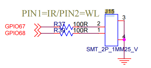
J15 GPIO (2P / 1.25mm)
| Pin | Signal | Note |
|---|---|---|
| 1 | GPIO68 | IR — PIR human-detection wake input (active low; level to be confirmed at product level) |
| 2 | GPIO67 | WL — white-light fill enable output |
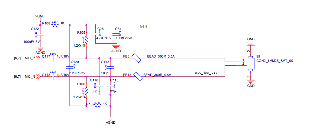
J1 MIC (2P / 1.25mm)
| Pin | Signal | Note |
|---|---|---|
| 1 | MIC_P | Microphone + (isolated through bead FB3) |
| 2 | MIC_N | Microphone − (isolated through bead FB4) |
J11 AUDIO (2P / 1.25mm)
| Pin | Signal | Note |
|---|---|---|
| 1 | VO+ | Amplifier output + |
| 2 | VO- | Amplifier output − |
CON5 IRCUT (2P / 1.25mm)
| Pin | Signal | Note |
|---|---|---|
| 1 | IROA | Filter driver A |
| 2 | IROB | Filter driver B |
J8 BOOT (2P)
| Pin | Signal | Note |
|---|---|---|
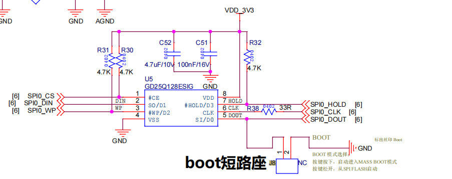
| 1 | BOOT_OUT | Boot mode select output; shorting it starts MASS BOOT mode (releasing the button boots normally from SPI flash) |
| 2 | GND | Ground |
CON6 MOTOR_1 (5-pin / Molex 53398, horizontal)
| Pin | Signal | Note |
|---|---|---|
| 1 | H_MB1 | Horizontal motor H-bridge output 1 |
| 2 | H_MB2 | Horizontal motor H-bridge output 2 |
| 3 | H_MB3 | Horizontal motor H-bridge output 3 |
| 4 | H_MB4 | Horizontal motor H-bridge output 4 |
| 5 | MOTOR_5V | Motor 5 V supply |
CON8 MOTOR_2 (5-pin / Molex 53398, vertical)
| Pin | Signal | Note |
|---|---|---|
| 1 | V_HB1 | Vertical motor H-bridge output 1 |
| 2 | V_HB2 | Vertical motor H-bridge output 2 |
| 3 | V_HB3 | Vertical motor H-bridge output 3 |
| 4 | V_HB4 | Vertical motor H-bridge output 4 |
| 5 | MOTOR_5V | Motor 5 V supply |
J5 BAT CHRG_EN (5P)
| Pin | Signal | Note |
|---|---|---|
| 1 | VBUS | 5 V input rail (from VCC_5V / solar panel through the charge IC) |
| 2 | GND | Ground |
| 3 | V_SYS | System power rail (output after switching between external supply and battery) |
| 4 | CHRG_EN | Charge enable (through series R34 100R) |
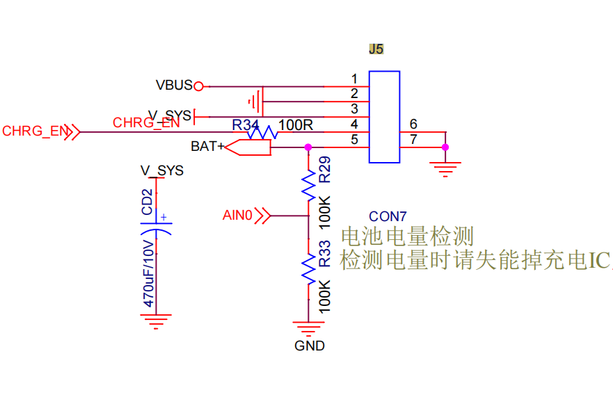
| 5 | BAT+ | Battery positive connection, also divided down to AIN0 for battery level sensing |
J10 AK_USB (4P)
| Pin | Signal | Note |
|---|---|---|
| 1 | GND | Ground |
| 2 | AK_DP | USB 2.0 D+ |
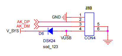
| 3 | AK_DM | USB 2.0 D− |
| 4 | VCC_5V | 5 V supply |
J12 MIPI / I2C0 / CSI2 (26P)
| Pin | Signal | Note |
|---|---|---|
| 1 | GND | Ground |
| 2 | MIPI_DP3 | MIPI data differential pair 3 + |
| 3 | MIPI_DN3 | MIPI data differential pair 3 − |
| 4 | GND | Ground |
| 5 | MIPI_DP4 | MIPI data differential pair 4 + |
| 6 | MIPI_DN4 | MIPI data differential pair 4 − |
| 7 | GND | Ground |
| 8 | GND | Ground |
| 9 | GND | Ground |
| 10 | MIPI_DP5 | MIPI data differential pair 5 + |
| 11 | MIPI_DN5 | MIPI data differential pair 5 − |
| 12 | GND | Ground |
| 13 | I2C0_SDA | I2C0 data (sensor configuration) |
| 14 | I2C0_SCL | I2C0 clock (sensor configuration) |
| 15 | CSI1_PWM | Fill-light PWM dimming (white light / infrared brightness) |
| 16 | LED_CON | Status indicator control |
| 17 | CSI2_RST / I2C2_SDA | Secondary sensor reset / I2C2 data (shared) |
| 18 | GND | Ground |
| 19 | CSI2_SCLK | Secondary sensor clock |
| 20 | GND | Ground |
| 21 | GND | Ground |
| 22 | VCC_5V | 5 V supply |
| 23 | VCC_5V | 5 V supply |
| 24 | VCC_5V | 5 V supply |
| 25 | GND | Ground |
| 26 | GND | Ground |
J4 4G_ANT (IPEX)
| Pin | Signal | Note |
|---|---|---|
| 1 | ANT_MAIN | 4G module main antenna (RF trace through π matching) |
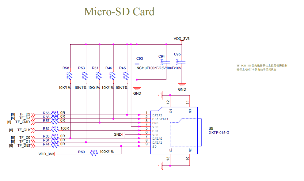
J3 TF Card (Micro SD, XKTF-015-G)
| Pin | Signal | Note |
|---|---|---|
| 1 | TF_D2 | Data line 2 |
| 2 | TF_D3 | Data line 3 |
| 3 | TF_CMD | Command |
| 4 | VDD_3V3 | 3.3 V supply (100R in series) |
| 5 | TF_CLK | Clock |
| 6 | TF_D0 | Data line 0 |
| 7 | TF_D1 | Data line 1 |
| 8 | TF_DET | Card detect (can act as an insertion event source in AOV) |
| 9 | GND | Ground |
5 Main controller specifications (KM01)
The KM01D and KM01N chips are designed for smart terminals such as IoT cameras and fit a wide range of AIoT scenarios including object detection, object tracking, face recognition and intelligent video surveillance. Built around an ARM926EJ-S core, they integrate a neural processing unit (NPU), an image signal processor (ISP) and H.265/H.264 video encoders, delivering high-quality image processing and high-compression video encoding while keeping power consumption low. Both chips support secure boot to protect firmware integrity and runtime safety. UART, TWI, SPI, I2S, MMC/SD/SDIO, Ethernet MAC and USB 2.0 peripherals make them highly extensible and easy to adapt to a wide variety of end products.
| Category | Parameter |
|---|---|
| CPU | 32-bit RISC CPU (ARM926EJ-S), up to 900 MHz |
| Memory | Built-in 512 Mibit / 1 Gibit DDR2 SDRAM |
| Neural processing unit | Object detection/tracking, face detection/recognition and other algorithms |
| Camera | MIPI and DVP interfaces, two CIS inputs supported |
| Image signal processor | Auto white balance, auto exposure, auto focus; gamma correction; bad-pixel correction; 3D/2D noise reduction; edge enhancement |
| Image signal pre-processor | 3 independent channels; mirroring and image flipping; OSD and rectangle drawing |
| Video encoder | H.265/H.264 encoder up to 3072×2048; JPEG encoder up to 16384×8192 |
| Audio codec | 1 × 22-bit Sigma-Delta DAC; 1 × 16-bit Sigma-Delta ADC |
| Peripheral interfaces | MMC/SD/SDIO, USB 2.0, Ethernet, TWI, UART, SPI, I2S |
| Security engine | Secure boot; AES/DES/3DES; AES256 decryption; RSA2048 signature verification; SHA256 |
| Package | QFN88 |
6 4G module specifications (ML120H)
In an AOV design the 4G module is the biggest power consumer and the component that implements the “send clips only, never the whole stream” policy. The board carries a Cat.1 bis module rather than Cat.4 — enough bandwidth for clip upload.
| Item | Parameter |
|---|---|
| Model | ML120H (schematic label le270-cn) |
| Standard | LTE Cat.1 bis (FDD + TDD) |
| Bands | FDD: B1 / B3 / B5 / B8; TDD: B34 / B38 / B39 / B40 / B41 |
| Dimensions | 15.8 mm × 17.7 mm × 2.2 mm |
| Package | LCC + LGA |
| Supply voltage | 3.4 V to 4.3 V (3.8 V typical); the board feeds it from VDD_3V3 |
| Data rate | FDD: 10 Mbps downlink / 5 Mbps uplink; TDD: 7.5 Mbps downlink / 1 Mbps uplink |
| Power consumption | Power off 55 uA; sleep 0.41 mA; standby 5.64 mA |
| Operating temperature | Normal -35 °C to +75 °C; extended -40 °C to +85 °C |
| Protocols | TCP / UDP / HTTP (S) / FTP / MQTT / SSL / TTS / FOTA |
| Interfaces | SIM ×1 (1.8 V / 3.0 V), USB 2.0 ×1, UART main + debug + auxiliary ports, I2C ×2, SPI ×2, ADC ×2, GPIO, Audio ×1, PWM ×2 |
| Antenna | Main antenna ANT_MAIN (J4 IPEX, π matching) |
| Certification | RoHS / CCC / SRRC (subject to the mass-production version) |
Selection note: Cat.1 uplink bandwidth is limited (FDD 5 Mbps / TDD 1 Mbps), so AOV event clip upload has to use H.265 with a key-frame-first policy — do not design for “uploading the full stream”. TDD bands only give 1 Mbps uplink, so if the deployment area has TDD coverage only, the upload bitrate ceiling must be lowered further.
⚠ Model uncertain (must be confirmed before shipment): the π matching network in the schematic 4G antenna circuit is labelled ML120H le270-cn, but these two names refer to Cat.1 modules from two different vendors — the ML120H comes from Xiamen Cheerzing IoT (HiSilicon Hi2131 platform, 15.8 × 17.7 × 2.2 mm) and the LE270 from Fibocom (17.7 × 15.8 × 2.4 mm). The two are very close in size, bands and interfaces, so a single line in the schematic is not enough to tell which one is actually fitted.This table is filled in for the ML120H; if the part is actually an LE270, the bands (B1/3/5/7/8/20/28) and the supply limit (4.5 V) have to be corrected accordingly. Before shipment confirm against the silkscreen on the actual module or the BOM, and update this table to match.
7 Interface circuit notes
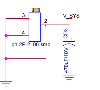
5V POWER (J13)
2.00 mm pitch SMD connector (ph-2P-2_00-smd); V_SYS is decoupled by a 470 uF/10 V capacitor (C3) before feeding the system.
DEBUG (J9)
UART0_RXD / UART0_TXD each run through a 100 Ω series resistor (R24 / R52) before leaving the board; 3-pin / 1.25 mm SMD connector, GND straight to ground.
TF Card (J3)
Socket model XKTF-015-G; six signals are brought out, data and command each with a 0 Ω series resistor and a 10K/1% pull-up; power is fed through R50 (100R) with 100 nF + 10 uF decoupling. Continuous AOV writing requires a high-endurance TF card.
GPIO (J15) — PIR wake-up and white-light fill
PIN1 = IR (PIR human infrared sensing), PIN2 = WL (white light); GPIO68 → IR and GPIO67 → WL, each through a 100 Ω series resistor. IR is the main wake source of the product and does not depend on 4G being online.
MIC (J1)
MIC_P / MIC_N differential input; the analog supply VCM3 is filtered by R108 (1K); bias resistors R105 / R106 (1.2K/1%); both lines leave the board isolated through beads FB3 / FB4 (300R / 0.5 A).
AUDIO (J11)
Uses an XA8002E (SOP8) amplifier; mute control SPK_EN; the differential HPOUT input runs through C402 (1 uF/6.3 V) plus the R402 (20K/1%) and R23 (100K/1%) bias network.
MOTOR (CON6 / CON8)
Two independent H-bridges: CON6 is horizontal (H_MB1~H_MB4) and CON8 is vertical (V_HB1~V_HB4); the drive supply is MOTOR_5V; the connectors are Molex 53398 5-pin / 1.25 mm.
BOOT (J8) and SPI flash
The SPI flash is a GD250Q128ESIG (128 Mbit); shorting BOOT starts MASS BOOT mode, and releasing the button boots normally from SPI flash. In production confirm that the jumper is not fitted.
BAT CHRG_EN (J5) — solar power and battery level sensing
Brings out VBUS / GND / V_SYS / CHRG_EN / BAT+; CHRG_EN leaves the board through R34 (100R); BAT+ is divided by R29 / R33 (100K each) and sampled on AIN0. This board does not include a charge IC.
MIPI / I2C0 / CSI2 (J12) — image input and fill-light dimming
Three MIPI differential pairs (MIPI_DP3/DN3, DP4/DN4, DP5/DN5); I2C0_SDA / I2C0_SCL are shared with CSI2_SCLK and CSI2_RST/I2C2_SDA; CSI1_PWM is used for fill-light PWM dimming.
4G_ANT (J4)
4G module ML120H (le270-cn); IPEX antenna connector, the RF trace runs through π matching to ANT_MAIN; the module has its own VDD_3V3 supply. The RF trace must hold a strict 50 Ω characteristic impedance.
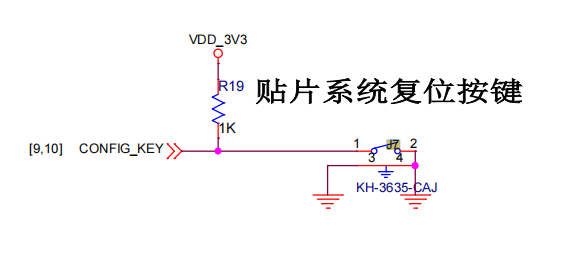
CONFIG_KEY (reset button)
Button model KH-3635-CAJ (SMD system reset button); CONFIG_KEY is pulled up to VDD_3V3 through R19 (1K) and pressing it pulls the line low to trigger a reset.
IRCUT (CON5)
Two outputs IROA / IROB with C106 (100 nF/25 V) across them for filtering; 2-pin / 1.25 mm SMD connector. Filter switching must be linked to the fill light and needs a debounce delay.
AK_USB (J10)
AK_DP / AK_DM USB 2.0 data pair; V_SYS feeds VUSB through D6 (DSK24 SOD-123); 4-pin SMD connector with ESD protection.
8 Key bill of materials (BOM extract)
| Designator | Part | Parameter / model | Function |
|---|---|---|---|
| U1 | SoC | ANYKA KM01 (D611) | Main controller |
| — | 4G module | ML120H (le270-cn) | LTE Cat.1 bis connectivity |
| U10 | Amplifier | XA8002E (SOP8) | Speaker driver |
| U5 | SPI FLASH | GD250Q128ESIG | 128 Mbit boot / firmware storage |
| — | Motor driver | Dual H-bridge | Horizontal + vertical PTZ |
| J3 | TF card socket | XKTF-015-G | Micro SD local storage |
| J4 | Antenna connector | IPEX | 4G antenna |
| J6 | Motor connector | Molex 53398 5P / 1.25mm | Horizontal + vertical motor |
| J13 | Power connector | ph-2P-2_00-smd | 5 V input |
| J5 | Battery connector | 5P | Battery / charge enable / battery level sensing |
| FB1 | Ferrite bead | 120R / 100M | V_SYS filtering |
| FB3 / FB4 | Ferrite bead | 300R / 0.5A | MIC signal isolation |
| D6 | TVS | DSK24 (SOD-123) | USB supply ESD protection |
| R29 / R33 | Resistor | 100K | Battery level divider |
| R34 | Resistor | 100R | CHRG_EN series resistor |
| R19 | Resistor | 1K | CONFIG_KEY pull-up |
| R38 | Resistor | 33R | BOOT signal series resistor |
| C3 | Capacitor | 470uF/10V | V_SYS bulk storage |
| C85 / C86 | Capacitor | 22uF/10V, 100nF/10V | V_SYS decoupling |
9 AOV external parts list
The board itself does not include the following parts; a product design has to add or select them:
| Category | External part | Connects to this board | Selection notes |
|---|---|---|---|
| Category | External part | Connects to this board | Selection notes |
| Energy | Solar panel | Via the charge IC → J13 (VBUS) | AOV draws more power than a PIR design; size the panel from the real power budget, usually no less than 5 W; MPPT recommended |
| Energy | Li-ion battery | J5 BAT+ | Derive the capacity from “average daily consumption × number of rainy days”; in cold regions you need low-temperature self-heating or a charge lockout |
| Energy | Charge / protection IC | J5 CHRG_EN | This board has no charge IC, so an external one is required; its CHRG_EN level definition must match |
| Sensing | PIR human detection | J15 PIN1 (IR / GPIO68) | The main AOV wake source; confirm the output level and hold time |
| Sensing | Image sensor | J12 MIPI differential pairs + I2C0 | Main + secondary camera; scenes with high low-light requirements need a large optical format / high-sensitivity model |
| Fill light | White-light LED board | J15 PIN2 (WL / GPIO67)+ J12 CSI1_PWM | High power draw; PWM dimming linked to the battery level is recommended |
| Fill light | Infrared fill-light board | J12 CSI1_PWM | Prefer the 940 nm wavelength to avoid green-light interference; works together with the IR-cut filter |
| Mechanical | IR-cut filter | CON5 (IROA/IROB) | Must be coaxial with the lens; watch the mechanical clearance when switching |
| Mechanical | Horizontal / vertical DC motor | CON6 / CON8 | Driven directly by the H-bridge; match the motor stall current and wire gauge |
| Storage | High-endurance TF card | J3 | 64 GB to 128 GB surveillance-grade recommended |
| Network | 4G antenna + feeder cable | J4 IPEX | The housing must keep antenna clearance; use a low-loss 50 Ω feeder |
| Acoustics | Microphone / speaker | J1 / J11 | Keep MIC traces away from the amplifier traces |
| Housing | IP65 or better protective housing | — | Mandatory for outdoor AOV; needs an antenna window and cooling vents |
10 Design notes
Battery life is a product parameter, not a board parameter: the board only provides the power interface and battery sampling. Real battery life comes from the solar panel wattage, battery capacity, charge/discharge policy, fill-light policy and recording duration together — always work out the power budget before quoting or discussing a project.
Power priority: 4G transmit > PTZ rotation > white-light fill > encoding and writing > always-on AI inference > deep sleep. When power runs short, cut from the back of this list forward and the core recording capability survives.
The always-on policy needs profiles: offer at least three profiles — “maximum saving / balanced / HD recording” — and let users pick per scenario (a busy doorway vs a backyard) instead of one fixed setting for everything.
Sleep and wake leakage current: in PIR standby the static leakage of the SoC and the 4G module sets the ceiling for “never runs out”; the module must really enter power-off / PSM rather than just network idle.
This board has no RTC: no standalone RTC chip is present on the board. If the product needs timed capture or timed upload while offline, add an external RTC on I2C, or rely on 4G network time (which stops working when offline).
Disable the charge IC before sensing battery level: the schematic states this explicitly — if the charge IC is not disabled, the divider reading is distorted.
The divider ratio needs calibration: R29/R33 = 100K/100K (1:2); at a full charge of 4.2 V, AIN0 sits at about 2.1 V, which is outside the usual ADC range, so the firmware must be calibrated against the real reference voltage and divider ratio.
The solar panel must have reverse-polarity and over-voltage protection: otherwise a rainy day or a reversed connection will burn the charge IC and then damage this board.
BOOT jumper: shorting J8 enters MASS BOOT programming mode; production firmware must confirm the jumper is not fitted, otherwise the board cannot boot from SPI flash nor be upgraded remotely.
MIPI differential pairs: they must be length-matched with continuous impedance and no vias or layer changes inside a pair; pins 8/9 and 16/17 can be cut directly to isolate debug segments.
Motor driver: H_MB/V_HB are H-bridge outputs and the motor is an inductive load; MOTOR_5V and the system 5 V must be decoupled separately, and the harness must stay away from the MIC and MIPI traces.
4G antenna and supply: the RF π matching must not be changed; transmit bursts draw large current, so leave headroom in the VDD_3V3 supply path and bulk capacitor.
TF card power: fed through R50 (100K) in series — check the voltage drop with fast high-capacity cards and move to a lower resistance if needed.
The pain point of AOV is “install it and nobody touches it again”: the device sits high up outdoors, so remote upgrade (4G FOTA), remote parameter change and remote reboot all have to be complete — otherwise every field issue means a site visit.
The TF card needs life monitoring: the firmware should read card health / bytes written and warn as end of life approaches; for PTZ cameras use cyclic overwrite rather than unlimited growth.
The battery needs health reporting: the product must report battery level, charging state and low-battery alarms to the cloud — once the battery fails, an AOV device goes offline completely.
Event clips and live preview need tiered throttling: Cat.1 uplink bandwidth is limited, so cap the concurrency and duration of live preview and give event upload priority.
11 Parameters still to be confirmed
The following items are not provided in the vendor documentation and must be filled in before the official external release:
| Item | Note |
|---|---|
| Item | Note |
| Measured product power consumption | Measured current in the always-on / event / sleep states, plus the 4G transmit peak current |
| Battery life estimate | To be produced from the solar panel wattage, battery capacity and rainy-day factor |
| Operating temperature range | Not specified by the vendor; take the intersection of the SoC, 4G module and battery ratings |
| Board weight | To be weighed (including the 4G module and flash) |
| 4G module and battery model confirmation | The schematic says ML120H (le270-cn); confirm the bands and certification of the shipping version with the module vendor |
| CHRG_EN polarity | Must match the selected charge IC |
| PIR level and hold time | Must match the selected PIR module |
| Fill-light circuit topology | What CSI1_PWM drives (white light / infrared / both) has to be confirmed at product level |
| Whether an RTC is fitted | Determines timed capture capability; a product-level decision |