IngenicT31+GC4653Network Module((Chinese version))
Project: Board Introduction | page_id: 888
| 4MP Camera | ||
|---|---|---|
| Category | Item | Specifications |
| Model | Main Chip | Ingenic T31ZX |
| Sensor | GalaxyCore GC4653 | |
| Capture Parameters | Lens | 4mm (optional 2.8mm, 6mm, 8mm and other lenses to suit different installation scenarios) |
| Sensor Type | GC4653 1/2.7'' 4MP sensor | |
| Minimum Illumination | 0.01lux/F1.2 (color), 0.01lux/F1.2 (black) | |
| Shutter | 1/3 second to 1/100.000 second | |
| Day/Night Switching | Supports hardware photosensor and software photosensor | |
| Video Parameters | Video Compression Standard | H.264/H.265 |
| Compression Output Bitrate | 128Kbps~8000Kbps | |
| Number of Streams | Dual stream | |
| Max Image Size | 2560x1440 | |
| Max Frame Rate | 25FPS | |
| Image Settings | Brightness, contrast, saturation, exposure, vertical flip, horizontal mirror | |
| Audio Parameters | Audio Output | Supported |
| Audio Input | Supported | |
| Network | Access Protocol | HTTP-FLV/RTSP/WEBRTC/RTMP/WS-FLV/WS-RAW/ONVIF GB/T28181 |
| Network Protocol | Supports TCP/IP, DHCP, DNS, NTP, RTSP, RTMP live streaming | |
| Wired Network | 1 RJ45 10M/100M Ethernet port | |
| Functions | Local Client | Supported |
| Network Access | Supported | |
| Local Upgrade | Supported | |
| OSD Overlay | Supported, more than 2 custom regions, supports time display | |
| Storage | Storage Function | Supports up to 512GB SD card storage |
| Recording Download | Supports local and remote recording download | |
| Recording Playback | Supports remote recording playback | |
| Others | Operating Temperature and Humidity | -10℃~50℃, humidity less than 95% |
| Power Consumption | 3W MAX |
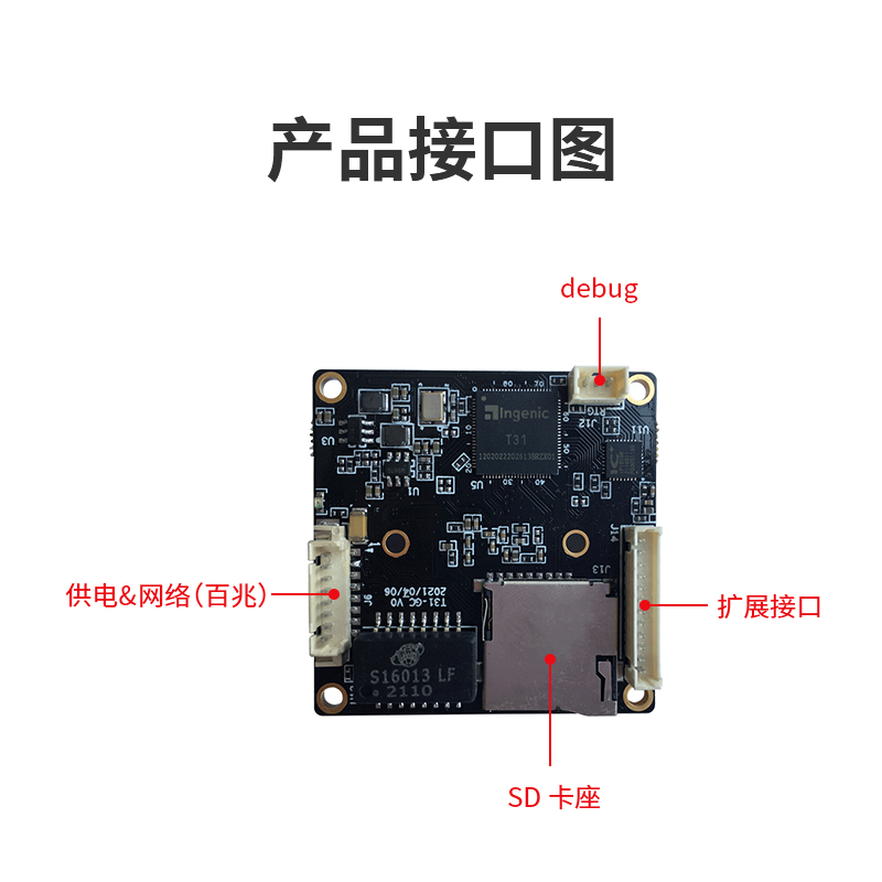
Board size: 38*38mm
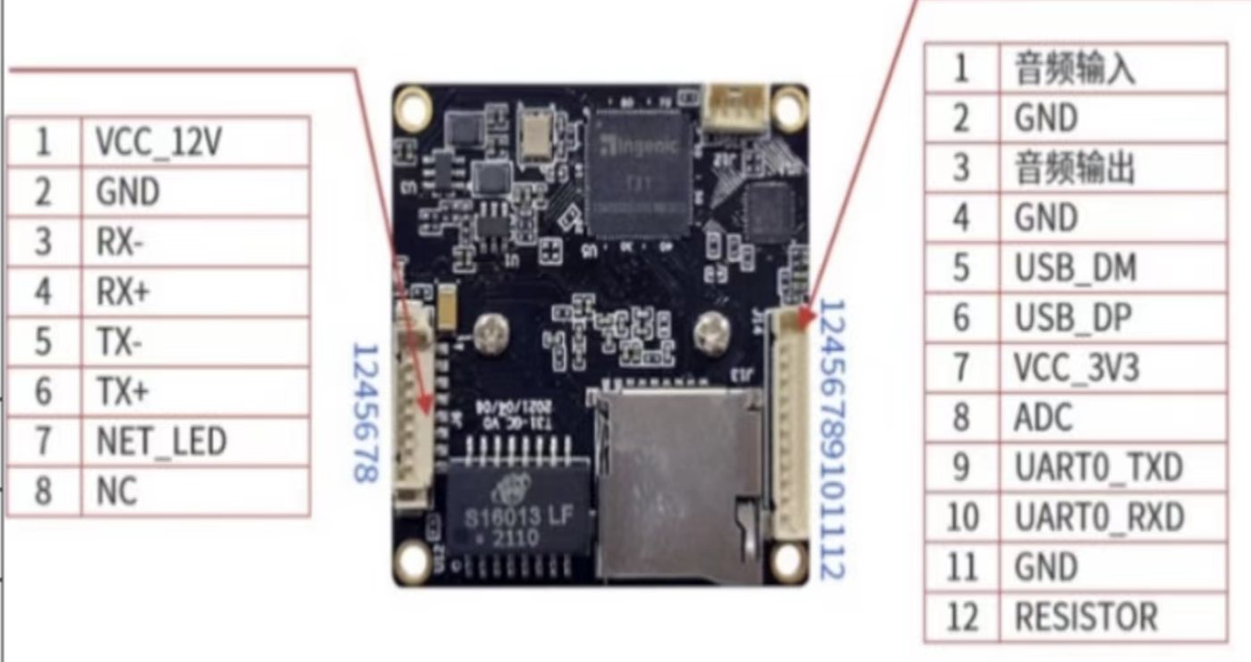
1. Chip Specifications
1. CPU
1.1 XBurst®-1 core
– XBurst® FPU instruction set supporting both single and double floating point format which are IEEE754 compatible
– XBurst® 9-stage pipeline micro-architecture, the operating frequency is 1.5GHz
· MMU
– 32-entry joint-TLB
– 8 entry instruction TLB
– 8 entry data TLB
· L1 Cache
– 32kB instruction cache
– 32kB data cache
· Hardware debug support
· 16kB tight coupled memory
· L2 cache
– 128kB unify cache
1.2 Video Processor Unit
· Support DVT HEVC/AVC/JPEG Encoder
· Support HEVC up to 20Mbit/s and AVC up to 40Mbit/s, maximum frame rate is 1920x1080@60fps or 2592x1900@25fps
· maximum size up to 2592X4096 resolution
1.3 Image Signal Processor
Dynamic/Static Defect Pixel Correction
Green Equalization
Black Level Correction
Lens Shading Correction
3A(Auto Exposure/White Balance/Focus)
Support Statistical Information Output(3A)
Adaptive Dynamic Range Compression
Demosaic
Sharpen Sharpen
Bayer Denoise
2D/3D Denosie
Color Noise Suppression
Lens Distortion Correction
2D Color Correction
3D Color Correction
Gamma Correction
Defog, WDR
3 Independent Image Scaler and Output
Crop, Mirror and Flip
Support Maximum Resolution: 2592X2048
1.4 Smart LCD Controller
Basic Features Basic Features Basic Features Basic Features
― Display size up to 800x600@60Hz,24BPP
― Smart LCD interface 6800(type A) and 8080(type B)
Color Supports
― Support up to 16,777,216 (16M) colors
Panel Supports
― transmit 565 by one cycle via SLCD 16bit data interface
― transmit 666 by two cycle via SLCD 9bit data interface
― transmit 565 by two cycle via SLCD 8bit data interface
― transmit 888 by three cycle via SLCD 8bit data interface
― Supports different size of display panel
― Supports internal DMA operation and direct write register operation
1.5 Video input
Support 8/10/12 bit RGB Bayer input
Support DVP,BT1120 (serial mode)/BT656/BT601 and MIPI CSI(2 lane up to 1.5Gbps)
Support maximum: 2592x1900@25fps
Support single-sensor input
1.6 Audio System
Integrated Audio codec
– 24 bits DAC with 93dB SNR
– 24 bits ADC with 92dB SNR
– Supportsignal-ended and differential microphone input and line input
– Automatic Level Control (ALC) for smooth audio recording
– Pure logic process: no need for mixed signal layers and less mask cost
– Programmable input and output analog gains
– Digital interpolation and decimation filter integrated
– Sampling rate 8K/12K/16K/24K/32/44.1K/48K/96KI
1.7 Memory Interface
Integrated 1G bit DDR on chip
Static memory interface
– Support Support 6 external chip selection CS6~1#. Each bank can be configured separately
– The size and base address of static memory banks are programmable
– Direct interface to 8-bit bus width external memory interface devices or external static memory to each bank. Read/Write strobe setup time and hold periods can be programmed and inserted in an access cycle to enable connection to low-speed memory
– Wait insertion by WAIT pin
– Automatic wait cycle insertion to prevent data bus collisions in case of consecutive memory accesses to different banks, or a read access followed by a write memory accesses to the same bank
1.8 System Functions
Clock generation and power management
– On-chip 12/24/48MHZ oscillator circuit
– One three-chip phase-locked loops (PLL) with programmable multiplier
– CCLK, HHCLK, H2CLK, PCLK, H0CLK, DDR_CLK, VPU_CLK frequency can be changed separately for software by setting registers
– SSI clock supports 50M clock
– MSC clock supports 100M clock
– Functional-unit clock gating
– Shut down power supply for P0, ISP, VPU, IPU
Timer and counter unit with PWM output and/or input edge counter
– Provide eight separate channels, six of them have input signal transition edge counter
– 16 -bit A counter and 16-bit B counter with auto-reload function every channel
– Support interrupt generati when the A counter underflow
– Three clock sources: RTCLK (real time clock), EXCLK (external clock input),PCLK APB Bus clock)selected with 1, 4, 16, 64, 256 and 1024 clock dividing selected
– Every channel has PWM output
OS timer controller
– 64-bit counter and 32-bit compare register
– Support interrupt generation when the counter matches the compare register
– Two clock sources: RTCLK (real time clock), HCLK (system bus clock) selected with 1, 4, 16, 64, 256 and 1024 clock dividing selected
Interrupt controller
– Total 64 interrupt sources
– Each interrupt source can be independently enabled
– Priority mechanism to indicate highest priority interrupt
– All the registers are accessed by CPU
– Unmasked interrupts can wake up the chip in sleep mode
– Another set of source, mask and pending registers to serve for PDMA
Watchdog timer
– Generates WDT reset
– A 16-bit Data register and a 16-bit counter
– Counter clock uses the input clock selected by software
PCLK, EXTAL and RTCCLK can be used as the clock for counter
The division ratio of the clock can be set to 1, 4, 16, 64, 256 and 1024 by software
Direct memory access controllers
– Support up to 32 independent DMA channels
– Descriptor or No-Descriptor Transfer mode compatible with previous JZ SoC
– Transfer data units: 1-byte, 2-byte, 4 byte, 4-byte, 16-byte, 32-byte, 64-byte, 128-byte
– Transfer number of data unit: 1 ~ 2^24-1
– Independent source and destination port width: 8-bit, 16-bit, 32-bit
– Fixed three priorities of channel groups: 0~3, highest; 4~11: mid; 12~31: lowest
– An extra INTC IRQ can be bound to one programmable DMA channel
SAR A/D Controller
– 1Channels
– Resolution: 10-bit
– Integral nonlinearity: ±1 LSB
– Differential nonlinearity: ±0.5 LSB
– Resolution/speed: up to 2MSPS
– Max Frequency: 24MHz
– Low power dissipation: 1.5 mW(worst)
– Support multi-touch detect
– Support write control command by software
– Single-end and Differential Conversion Mode
– Support external touch screen controller
– Pin Description
OTP Slave Interface
– Total 1024 bits. Lower 192bits are read only, other higher bits are read-able and write-able
1.9 Peripherals
General -Purpose I/O ports
– Each port can be configured as an input, an output or an ernate function port
– Each port can be configured as an interrupt source of low/high level or rising/falling edge triggering. Every interrupt source can be masked independently
– Each port has an internal pull-up pull-down resistor connected. The pull-up/down resistor can be disabled
– GPIO output 3 interrupts, each interrupt corresponds to the group, to INTC
SMB Controller SMB Controller SMB Controller
– Two-wire SMB serial interface – consists of a serial data line (SDA) and a serial clock (SCL)
– Two speeds
– Standard mode (100 Kb/s)
– Fast mode (400 Kb/s)
– Device clock is identical with pclk
– Programmable SCL generator
– Master or slave SMB operation
– 7-bit addressing/10-bit addressing
– 16-level transmit and receive FIFOs
– Interrupt operation
– The number of devices that you can connect to the same SMB-bus is limited only by the maximum bus capacitance of 400pF
– APB interface
– 2 independent SMB channels (SMB0,SMB1)
One High Speed Synchronous serial interfaces(SFC)
– 3 protocols support: National’s Microwire, TI’s SSP, and Motorola’s SPI
– transmit-only or receive-only operation
– MSB first for command and data transfer, and LSB first for address transfer
– 64 entries x 32 bits wide data FIFO
– one device select
– Configurable sampling point for reception
– Configurable timing parameters: tSLCH, tCHSH and tSHSL
– Configurable flash address wide are supported
– transfer formats: Standard SPI only
– two data transfer mode: slave mode and DMA mode
– Configurable 6 phases for software flow
Normal Speed Synchronous serial interfaces (SSI1)
– 3 protocols support: National’s Microwire, TI’s SSP, and Motorola’s SPI 3 protocols
– Full-duplex or transmit-only or receive-only operation
– Programmable transfer order: MSB first or LSB first
– 128 entries deep x 32 bits wide transmit and receive data FIFOs
– Configurable normal transfer mode or Interval transfer mode
– Programmable clock phase and polarity for Motorola’s SSI format
– Back-to-back character transmission/reception mode
– Loop back mode for testing
Three UARTs (UART0, UART1, UART2)
– Full-duplex operation
– 5-, 6-, 7- or 8-bit characters with optional no parity or even odd parity and with 1, 1½, or 2 stop bits
– 64x8 bit transmit FIFO and 64x11bit receive FIFO
– Independently controlled transmit, receive (data ready or timeout), line status interrupts
– Internal diagnostic capability Loopback control and break, parity, overrun and framing-error is provided
– Separate DMA requests for transmit and receive data services in FIFO mode
– Supports modem flow control by software or hardware
– Slow infrared asynchronous interface that conforms to IrDA specification
Two MMC/SD/SDIO controllers(MSC0, MSC1)
– Fully compatible with the MMC System Specification version 4.2
– Support SD Specification 3.0
– Support SD I/O Specification 1.0 with 1 command channel and 4 data channels
– Consumer Electronics Advanced Transport Architecture (CE-ATA – version 1.1)
– Maximum data rate is 50MBps
– Support MMC data width 1bit ,4bit and 8bit
– Built-in programmable frequency divider for MMC/SD bus
– Built-in Special Descriptor DMA
– Maskable hardware interrupt for SDIO interrupt, internal status and FIFO tatus
– 128 x 32 built-in data FIFO
– Multi-SD function support including multiple I/O and combined I/O and memory
– IRQ supported enable card to interrupt MMC/SD controller
– Single or multi block access to the card including erase operation
– Stream access to the MMC card
– Supports SDIO read wait, interrupt detection during 1-bit or 4-bit access
– Supports CE-ATA digital protocol commands
– Support Command Completion Signal and interrupt to CPU
– Command Completion Signal disable feature
– The maximum block length is 4096bytes
USB 2.0 USB interface
– Complies with the USB 2.0 standard for high-speed (480 Mbps) functions and with the On-The-Go supplement to the USB 2.0 specification
– Operates either as the function controller of a high-/full-speed USB peripheral or as the host/peripheral in point-to-point or multi-point communications with other USB functions
– Supports Session Request Protocol (SRP) and Host Negotiation Protocol(HNP)
– UTMI+ Level 3 Transceiver Interface
– Soft connect/disconnect
– 16 Endpoints
– Dedicate FIFO
– Supports control, interrupt, ISO and bulk transfer
Ethernet Media Access controller and interface
– 10, 100Mbps data transfer rates with the following PHY interfaces:
RMII interface to communicate with an external Fast Ethernet PHY
– Full -duplex operation:
IEEE 802.3x flow control automatic transmission of zero-quanta Pause frame on flow control input de-assertion
forwarding of received Pause frames to the user application
– Half-duplex operation:
– CSMA/CD Protocol support
– Frame bursting and frame extension in 100 Mbps half-duplex operation
– Preamble and start of frame data (SFD) insertion in Transmit path
– Preamble and SFD deletion in the Receive path
– Automatic CRC and pad generation controllable on a per-frame basis frame basis
– Automatic Pad and CRC Stripping options for receive frames
– Flexible address filtering modes, such as:
Up to 31 additional 48-bit perfect(DA) address filters with masks for each byte
64 -bit Hash filter for multicast and unicast (DA) addresses
Option to pass all multicast addressed frames
Promiscuous mode to pass all frames without any filtering for network monitoring
Pass all incoming packets (as per filter) with a status report
– Support Standard or Jumbo Ethernet frames with up to 2KB of size
– IEEE 802.1Q VLAN tag detection for reception frames
– MDIO master interface for PHY device configuration and management
– CRC replacement, Source Address field insertion or replacement, and VLAN insertion, replacement, and deletion in transmitted frames with pe-frame control
– Programmable watchdog timeout limit in the receive path
– Detect remote wake-up frames and AMD magic
Digital True Random Number Generator(DTRNG)
– Pure digital logic circuits
– True random number
– Interrupt mode and no interrupt mode
1.10 Bootrom
16KB Boot ROM memory
2. Interface Circuit Diagrams
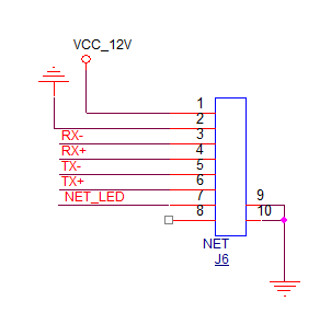
* 12V power supply + 100M network (8pin) x1
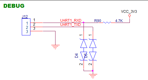
* Serial debug interface (3pin) x1
* Analog audio input + analog audio output + TTL serial port 1 + USB interface + GPIO + IR-CUT detection (12pin) x1
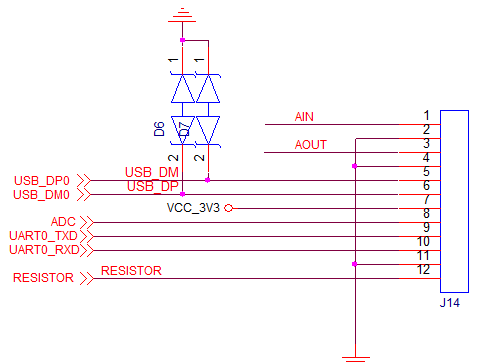
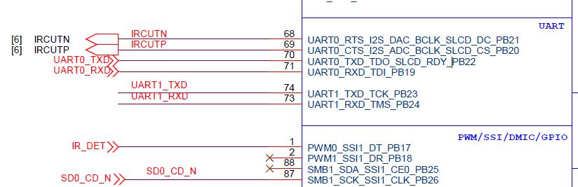
Main board wiring diagram
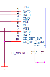
* Micro SD card slot x1
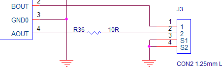
* IR-CUT interface x1
3. FAQ
| Question | Answer |
|---|---|
| 1. What is the focal length? | Development boards ship with a random focal length; the lens focal length is only fixed for bulk purchases. Options: 2.4mm/4mm/6mm |
| 2. What about the corresponding lens focal lengths? Different lenses have different ISP parameters, right? | The ISP parameters for 2.8, 4 and 6 have all been tuned |
| 3. Is the ISP source code provided? | Ingenic's ISP has no source code; the ISP has already been tuned by Ingenic |
| 4. T31 runs a Linux system, right? Does it support a touch screen? | Yes, it is a Linux system; touch screens are not supported |
| 5. Is a programmer included? | Flashing can be done directly via the serial port or the network |
| 6. Can the included development environment support the camera fast-boot resources? I need to develop secondary camera capture functions, so I need drivers for fast boot and snapshot. | No, fast boot is only supported through custom development and requires a customization fee. There are corresponding debug interfaces and an SDK, but you need to adapt it yourself |
| 7. Do you have a basic development environment and basic function examples? | Yes |
| 8. What materials are provided? Do you provide H.265 encoding and RTSP source code? | An SDK virtual machine is provided; there is no RTSP source code, but there are H.265 encoding examples |
| 9. Does it support remote wake-up? | No |
| 10. Is the camera on this development board external? | It is built-in; just install a lens |
| 11. Is there a USB data transfer port? Does USB support video signal input? | There is USB on the expansion connector; USB does not support video signal input |
| 12. How is distortion correction performed? Is it invoked from the settings menu? | Distortion correction is an official Ingenic feature and is included in the SDK |
| 13. What is the virtual machine password? What is the root password of this embedded system? Is there a CPU manual for the T31ZX? I want to see what internal resources it has | VM password: 123456; root has an empty password; the manual is in the SDK |
| 14. What are the differences between T31 and T40? | T40 supports intelligent analytics while T31 does not; only T40 has NPU computing power |
| 15. Does T31 support binocular? | No |
| 16. Does this support x1500 development? | No |
| 17. How does the Ingenic board connect to WiFi, USB or SDIO? Which WiFi chip is used? | USB. T31+imx307 cannot add 4G or WiFi modules; T31+GC4653 can add 4G and WiFi modules separately. The WiFi chip is 8188; adding a WiFi module costs an extra 50 CNY |
| 18. Can the firmware be modified? Is the network model a server or a client? How is customization charged? Can exposure parameters be set individually? Can the hardware be customized? Does the customization fee include software? Is there a basic SDK? | The firmware can be customized; RTSP is a server; the customization fee is evaluated based on your requirements; exposure parameters can be set individually; the hardware can be customized; the customization fee does not include software source code, but driver adaptation is possible; a basic SDK is available |
| 19. Can you customize solutions? For example, with T31, is there a matching APP and server? | Solutions can be customized, and the matching APP can also be customized |
| 20. Does the server need to be rented? How is it provided? | The server is billed by traffic according to your needs; generally, customization customers set up their own servers |
| 21. Is a mobile APP source code example provided? | No APP source code is available |
| 22. Are u-boot and the Linux kernel provided? | Yes, they are provided |
| 23. Is the board IP 192.168.0.10? Why can't I ping it? | You need to flash the firmware yourself; the default firmware inside is a test firmware |
| 24. How high a temperature can this camera withstand? | 80 degrees |
| 25. Does it support reading TF card data via USB? | It supports reading TF card data; there is a TF card slot |
| 26. Does it support MIPI? | Yes |
| 27. What is the exact Linux version? How large is the flash? How much built-in memory does T31 have? | Linux version: 4.4.49, this package is in the SDK; flash: NOR flash, size 16M; built-in memory 128M |
| 28. With 16M flash, how much space is left after running the camera demo? | The official u-boot is within 250KB, the kernel within 2M, and the filesystem 2-3M; the rest is space you can use, and the compiled demo program is very small |
| 29. Does it support auto exposure and auto white balance? | No. The board supports them but the sensor does not; the original sensor is soldered on the board, so custom hardware is required |
| 30. Can it achieve stable image output within 200ms? | This is a development board; its performance depends on the software you write. If you need to test performance, we recommend buying our finished camera product |
| 31. Is GB28181 code provided in the materials? | No |
| 32. Are the schematic and PCB included? | No, the schematic and PCB are charged separately, 8000 in total |
| 33. Can it communicate with another board via serial port? | Yes, there is a debug serial port |
| 34. Does this development board support root? Is the root password provided? | Yes, it is supported and provided |
| 35. Can the expansion connector support a microphone, speaker, PWM and two GPIOs at the same time? | The others are fine, but only one GPIO is supported |
| 36. Is there an SLCD display interface? | No |
| 37. Is the Linux source code available? | The Linux kernel source code is in the SDK |
| 38. What is the pin pitch? | 1.25mm |
| 39. Is there a version with a reserved SDIO interface for connecting an SDIO WiFi module? | No, only USB |
| 40. Is software source code provided for customization? | No. All customization refers to custom software features; software source code is not provided. All software source code is not for sale, and even if purchased the price would be very high, starting at least at 500,000 |
| 41. Is there a fast-boot demo in the T31 board materials? | No |