IngenicT40Dualmipi4GWFIBoard
Project: Board Introduction | page_id: 897
| T40 Dual-Sensor 4G WIFI Board | |
|---|---|
| Order Model | T40-N-DSNS-4G-WIFI |
| CPU | XBurst®2 up to 1.2GHz, Dual Core |
| Memory | Built-in 2Gb |
| MCU | 600MHz RISC-V coprocessor, 32bit, in-order 5-stage pipeline core |
| AI | Supports int16/int8/int4/int2, 8TOPS |
| Video Encoding | Supports H.265/H.264 encoding, max resolution 1920x1080@30fps |
| Camera | Supports dual cameras (GC2053) |
| Audio Input | Analog audio, sampling rate: 8K/12K/16K/24K/32K/44.1K/48K/96K |
| Serial Port | RS232x1, RS485x1 |
| Storage | Supports TF card expansion, up to 512GB |
| Network | RJ45 10/100M, CAT4 4G, 2.4/5G WiFi |
| Operating Temperature | 0 to 70℃ |
| Service Life | Continuous operation lifespan of more than 3 years |
1. Product Images
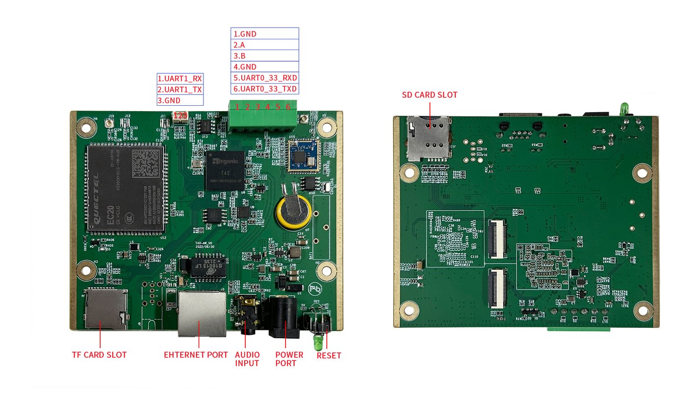
2. Chip Introduction
Features
• 1.2GHz XBurst2 dual-core CPU
• 4K (2160P) real-time video encoding
• 8T OPS AIE (NPU) hardware computing power
• Triple camera input, binocular vision
• Magik one-stop algorithm development platform
• Rich interfaces, 1080P display
1 CPU
XBurst®2 up to 1.2GHz, Dual Core, Dual-issue, high performance and low power implementation
of MIPS32 ISA R5
MIPS32 ISA R5 plus Ingenic SIMD512 ISA
Dual-issue, superscalar, super pipeline with Simultaneous Multi-Threading(SMT)
Two
hardware threads per physical core
Quad
instruction fetches per cycle
Dual
issue instructions per cycle per thread
32K L1 D cache + 32K L1 I cache, 128~1024K L2 cache
High-performance Floating-point Unit and SIMD Engine: FSE
32x512-
bit register set, 512-bit loads/stores to/from SIMD unit
IEEE-
754 2008 compliant
Programmable Memory Management Unit(MMU)
1st
level mini-TLBs(MTLBs)-8x2 entry instruction TLB, 16x2 entry data TLB
2nd
level TLBs:32x2 entry VTLB, 256x2 entry 4-way set associative FTLB
The XBurst®2 processor system supports little endian only
2 MCU
600MHz RISC-V coprocessor
32bit, in-order, 5-stage pipeline core
32K L1-cache and 32K L1 D-cache
RV32IM instruction set architecture
3 AI Engine
Built-in neural network accelerator
Typical Performance: 8TOPS
Support int16/int8/int4/int2 bit width
Shared 1MB memory pool
Magik AI algorithm develop platform available
4 AI Co-Processing Unit(AIU)
Color conversion
Resize
Hardware matrix operations
5 Video Processor Unit(VPU)
Support H.264/H.265/JPEG combo Encoder
Real-time H.256/H.264 encoding capabilities:3840x2160@30fps
Support maximum resolution up to 4096x4096
JPEG snapshot at 8 megapixels
6 Image Signal Processor(ISP)
Support up to 3 sensors
Support MIPI and DVP interface sensor
Support maximum resolution 3840x2160
3A (Auto Exposure/Auto White Balance/Auto Focus) and able to output the statistical
information
Green equalization
Black level correction
Lens Shading Correction
Lens Distortion Correction
Dynamic/Static Defect pixel correction
Demosaic
2D/3D Color Correction
Gamma Correction
Brightness/Contrast/Saturation/Hue Adjustment
Adaptive Dynamic Range Compression
Defog, WDR
Adaptive Local Contrast Enhancement
Sharpen
2D/3D Denoise
Chroma Noise Reduction
3 Independent Image Scale Up/Down Engine
Crop, Mirror and Flip
7 Display Process Controller(DPU)
MIPI-DSI4 interface
― Display size up to 1920x1080@60Hz
SLCD controller
― Display size up to 640x480@60Hz,24BPP
― Support different size of display panel
RGB controller
― Display size up to 1280x720@60Hz,24BPP
― Supports input format, ARGB8888, ARGB1555, RGB888, RGB565, RGB555, YUV422,
YUV420
― Support 4 modes parallel interface, 24-bit, 18-bit, 16-bit and 8-bit(third times)
― Support frame buffer crop and dither
8 Video Input and Output
Video Input
– Support 8/10/12 bit RGB Bayer input
– Support DVP, BT1120(serial model)/BT656/BT601
– Support MIPI CSI (lane up to 1.5Gbps, and support one 4-Lane or two 2-Lane sensor)
– Support maximum:3840x2160@30fps
– Support up to 3 sensor inputs (DVP/BT, two CSI 2lane)
Video output
– Support BT656 serial/parallel mode
– Support BT1120 serial/parallel mode
– Support MIPI DSI 4lane
9 Audio System
Integrated Audio Codec
– 24 bits DAC with 93dB SNR
– 24 bits ADC with 92dB SNR
– Support signal-ended and differential microphone input and line input
– Automatic Level Control (ALC) for smooth audio recording
– Pure logic process: no need for mixed signal layers and less mask cost
– Programmable input and output analog gains
– Digital interpolation and decimation filter integrated
– Sampling rate 8K/12K/16K/24K/32/44.1K/48K/96K
Digital MIC controller
– 16 bits data interface and 20bit precision internal controller
– SNR:90dB, THD:-90dB @ FS -20dB
– Linear high pass filter include. Attenuation: -2.9dB@100Hz, -22dB@27Hz, -36dB@10Hz
– Low power voice trigger when waiting to start talking
– 1/2/3/4 channel digital MIC support
– Support voice data pre-fetch when trigger enable and the data interface disable, but do
not increase the power dissipation
– Sample frequency supported: 8K, 16K
– Support low power mode, user for decrease DMIC sensor and DMIC controller power
dissipation
Standard Audio I2S Interface
– 16,20 and 24 bit audio sample data sizes supported, 16 bits packed sample data is
supported
– DMA transfer mode supported
– Stop serial clock supported
– Support mono PCM data to stereo PCM data expansion on audio play back
– Support endian switch on 16-bits normal audio samples play back
– Internal programmable or internal serial clock and optional system clock supported for
I2S or MSB-Justified format
– Two FIFOs for transmit and receive respectively
– Support different sample rate for transmit and receive
– Support echo cancellation function in the condition of the same sample rate in transmit
and receive
10 Memory Interface
Support up to size 2GB KGD and DDR2, DDR3, DDR3L
11 System Functions
Clock generation and power management
– On-chip 12/24/48MHZ oscillator circuit
– One four-chip phase-locked loops (PLL) with programmable multiplier
– CCLK, HHCLK, H2CLK, PCLK, H0CLK, DDR_CLK, VPU_CLK frequency can be
changed separately for software by setting registers
– SSI clock supports 50M clock
– MSC clock supports 100M clock
– Functional-unit clock gating
– Shut down power supply for CPU, ISP, VPU, IPU
Timer and counter unit with PWM output and/or input edge counter
– Provide eight separate channels, six of them have input signal transition edge counter
– 16-bit A counter and 16-bit B counter with auto-reload function every channel
– Support interrupt generation when the A counter underflow
– Three clock sources: RTCLK (real time clock), EXCLK (external clock input), PCLK (APB
Bus clock) selected with 1, 4, 16, 64, 256 and 1024 clock dividing selected
– Every channel has PWM output
OS timer controller
– 64-bit counter and 32-bit compare register
– Support interrupt generation when the counter matches the compare register
– Two clock sources: RTCLK (real time clock), HCLK (system bus clock) selected with 1, 4,
16, 64, 256 and 1024 clock dividing selected
Interrupt controller
– Total 64 interrupt sources
– Each interrupt source can be independently enabled
– Priority mechanism to indicate highest priority interrupt
– All the registers are accessed by CPU
– Unmasked interrupts can wake up the chip in sleep mode
– Another set of source, mask and pending registers to serve for PDMA
Watchdog timer
– Generates WDT reset
– A 16-bit Data register and a 16-bit counter
– Counter clock uses the input clock selected by software
PCLK, EXTAL and RTCLK can be used as the clock for counter
The division ratio of the clock can be set to 1, 4, 16, 64, 256 and 1024 by software
Direct memory access controllers
– Support up to 32 independent DMA channels
– Descriptor or No-Descriptor Transfer mode compatible with previous JZ SoC
– Transfer data units: 1-byte, 2-byte, 4-byte, 16-byte, 32-byte, 64-byte, 128-byte
– Transfer number of data unit: 1 ~ 224 - 1
– Independent source and destination port width: 8-bit, 16-bit, 32-bit
– Fixed three priorities of channel groups: 0~3, highest; 4~11: mid; 12~31: lowest
– An extra INTC IRQ can be bound to one programmable DMA channel
SAR A/D Interface
– 4 single-ended input channels and 4 Standard I/O cell multiplexed
– 12-bit resolution, up to 2MS/s sampling rate
– DNL<1LSB,INL<2LSB
– Max Frequency: 24MHz
– Current consumption:2.5mA@2MS/s
OTP Slave Interface
– Total 2048 bits. and used as 1024 bits for safe
Power On Reset(POR)
– Provides reliable reset function for general applications
– Monitor 1.8V supply for IO and 0.9V for core
– Typical 1.35V threshold for 1.8V supply
– Typical 0.6V threshold for 0.9V supply
12 Peripherals
General-Purpose I/O ports
– Input/output/function port configurable
– Low/high, rising/falling edge triggering. Every interrupt source can be masked
independent
– four interrupts, each interrupt corresponds to the group, to INTC
Four I2C Controller(SMB0, SMB1, SMB2, SMB3)
– Two-wire I2C serial interface – consists of a serial data line (SDA) and a serial clock
(SCL)
– Three speeds mode
Standard mode (100 Kb/s)
Fast mode (400 Kb/s)
High speed mode(3.4Mb/s)
– Programmable SCL generator
– Master or slave I2C operation
– 7-bit addressing/10-bit addressing
– The number of devices that you can connect to the same I2C-bus is limited only by the
maximum bus capacitance of 400pF
One High Speed Synchronous serial interfaces (SFC)
– 3 protocols support: National’s Microwire, TI’s SSP, and Motorola’s SPI
– transmit-only or receive-only operation
– MSB first for command and data transfer, and LSB first for address transfer
– 64 entries x 32 bits wide data FIFO
– one device select
– Configurable sampling point for reception
– Configurable timing parameters: tSLCH, tCHSH and tSHSL
– Configurable flash address wide are supported
– transfer formats: Standard SPI only
– two data transfer mode: slave mode and DMA mode
– Configurable 6 phases for software flow
Normal Speed Synchronous serial interfaces (SSI0, SSI1)
– 3 protocols support: National’s Microwire, TI’s SSP, and Motorola’s SPI
– Full-duplex or transmit-only or receive-only operation
– Programmable transfer order: MSB first or LSB first
– 128 entries deep x 32 bits wide transmit and receive data FIFOs
– Configurable normal transfer mode or Interval transfer mode
– Programmable clock phase and polarity for Motorola’s SSI format
– Back-to-back character transmission/reception mode
– Loop back mode for testing
Four UARTs (UART0, UART1, UART2,UART3)
– Full-duplex operation
– 5-, 6-, 7- or 8-bit characters with optional no parity or even or odd parity and with 1, 1½,
or 2 stop bits
– 64x8 bit transmit FIFO and 64x11bit receive FIFO
– Independently controlled transmit, receive (data ready or timeout), line status interrupts
– Internal diagnostic capability Loopback control and break, parity, overrun and
framing-error is provided
– Separate DMA requests for transmit and receive data services in FIFO mode
– Supports modem flow control by software or hardware
– Slow infrared asynchronous interface that conforms to IrDA specification
Two MMC/SD/SDIO controllers (MSC0, MSC1)
– All support eMMC 5.1(command queueing Engine)
– Support SD Specification 3.0
– Support SD I/O Specification 1.0 with 1 command channel and 4 data channels
– Consumer Electronics Advanced Transport Architecture (CE-ATA – version 1.1)
– Maximum data rate is 104MBps
– Both support MMC data width 1bit, 4bit
– Single or multi block access to the card including erase operation
– The maximum block length is 4096bytes
USB 2.0 OTG interface
– Complies with the USB 2.0 standard for high-speed (480 Mbps) functions and with the
On-The-Go supplement to the USB 2.0 specification
– Operates either as the function controller of a high- /full-speed USB peripheral or as the
host/peripheral in point-to-point or multi-point communications with other USB functions
– Supports Session Request Protocol (SRP) and Host Negotiation Protocol (HNP)
– UTMI+ Level 3 Transceiver Interface
– Soft connect/disconnect
– 16 Endpoints
– Dedicate FIFO
– Supports control, interrupt, ISO and bulk transfer
Ethernet Media Access controller
– 10/100 Mbps operation
– Supports MII and RMII PHY interfaces
– Support IEEE 1588-2002
Digital True Random Number Generator(DTRNG)
– Pure digital logic circuits
– True random number
– Interrupt mode and no interrupt mode
13 Bootrom
22kB Boot ROM memory
3. Interface Circuits
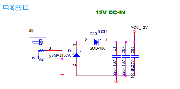
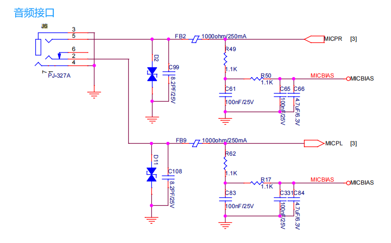
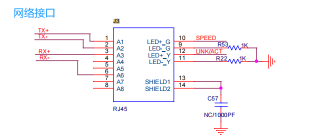
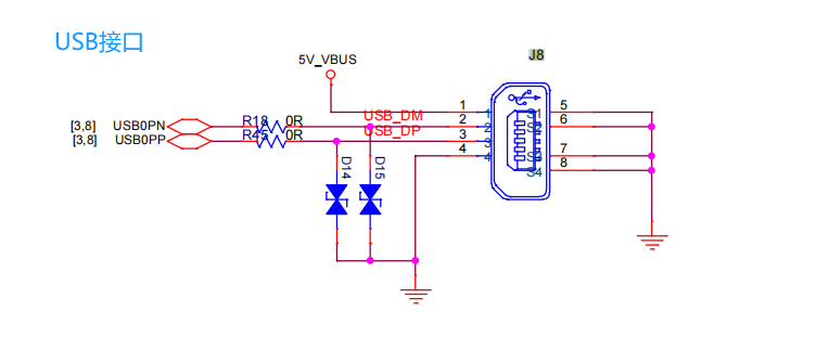
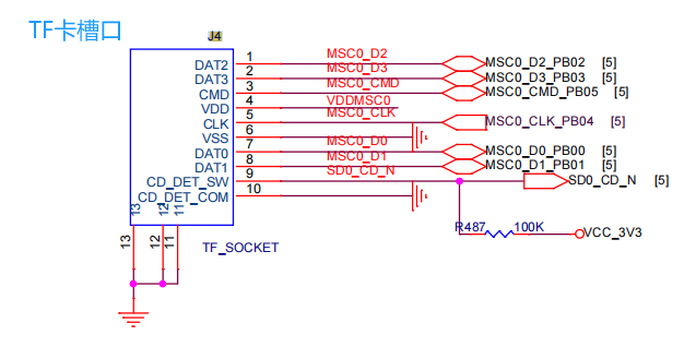
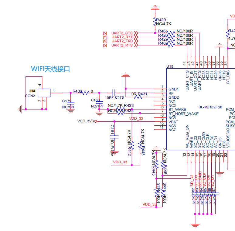
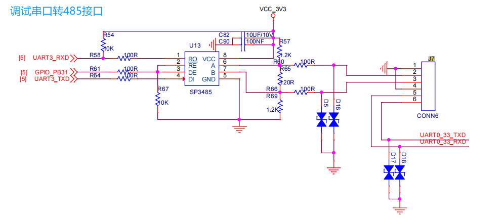
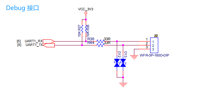
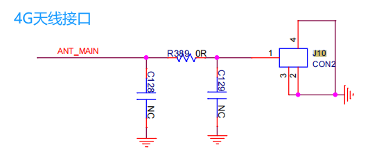
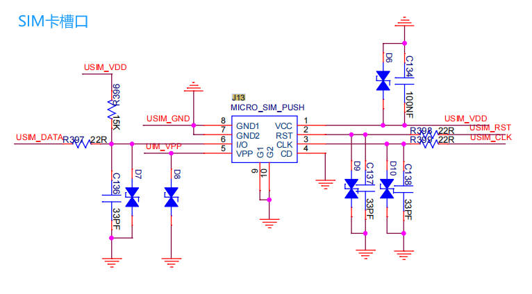
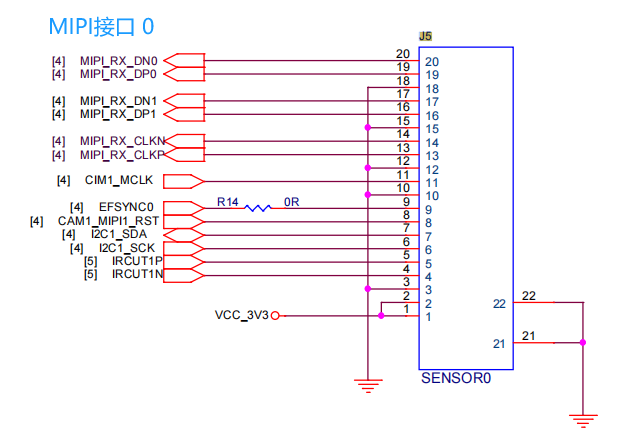
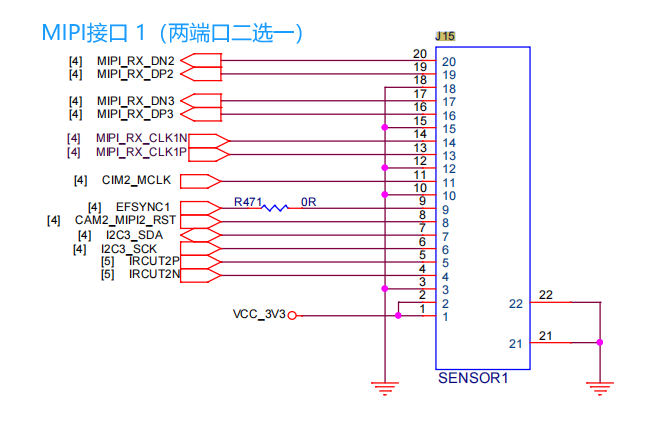
4. FAQ
| Question | Answer | ||
|---|---|---|---|
| 1. Is there a 4G module? Does the 4G module support APN? | T40XP has 4G and WiFi modules (WiFi module model bl-8189); T40ipc does not have 4G or WiFi modules. The 4G module supports APN | ||
| 2. Does it support battery power? | Yes, but battery power requires an additional boost circuit | ||
| 3. Is there an example for camera capture and 4G transmission? | You need to write the software yourself; there is no ready-made transmission example | ||
| 4. What materials are provided? | Official SDK, virtual machine, sample programs, hardware interface diagrams (debug serial port, MIPI pin order, etc.) | ||
| 5. Does the firmware on the board support recording and image preview? | The program on the board is our test program, which supports recording and image preview, but the source code is not provided. For your own development you need to refer to the code in the virtual machine | ||
| 6. Is the SDK the original unmodified SDK? | Yes | ||
| 7. Is the sensor driver provided? | Yes | ||
| 8. What is the power consumption of the T40 board? | It is relatively low, within 2W | ||
| 9. Does it support binocular video stitching? | Seamless stitching is not supported; yolov5 is supported | ||
| 10. Is there a tutorial or example for loading your own AI model? | Yes | ||
| 11. For secondary development of loading your own model, is there a GUI? | No GUI | ||
| 12. For video object detection, how many frames can it reach? | About 15 fps | ||
| 13. What system is built in? What development environment is supported? | Embedded Linux; it can only run embedded Linux | ||
| 14. What data type is the 8TOPS network? | int2 | ||
| 15. Does this board have no LCD interface? | Currently it has no LCD interface | ||
| 16. Does this development board come with a pre-downloaded image? | Yes | ||
| 17. Does the board come with example source code and schematics? Can the official schematic be provided? | The schematic is currently not provided and is charged separately — 2500 for the schematic alone, in PDF format; example source code is available; the official schematic can be provided | ||
| 18. Can the official SDK run all the functions of this board? | Some functions need to be developed by yourself. The development board is for development and requires some background. We provide driver source code, and our sample program can display both video channels. But if you want to run it yourself, you also need to compile the samples and load the drivers yourself | ||
| 19. Can the current board connect three sensors? | No, only two. Currently there is no version that supports three; theoretically three is possible, but the board would need to be redesigned | ||
| 20. Can T40 with dual sensors reach 60fps? | It can only reach 30FPS | ||
| 21. Does it support Bluetooth? | No, neither T40XP nor T40ipc supports Bluetooth | ||
| 22. Does T40 support MIPI screens? | No. The chip itself supports it, but our board does not | ||
| 23. Is there a T40N board? | Not at the moment | ||
| 24. Does the test firmware support GB28181? Is it the 2016 or 2022 version? | GB28181 is supported, 2016 version | ||
| 25. Does it have a DVP interface? | No, but it can be customized | ||
| 26. Is the lens mount of this module M12x0.5? | Yes, it is an M12 lens with a 0.5 thread pitch | ||
| 27. Does it have IR-CUT? | T40+GC2053 does not, T40+GC4653 does | ||