君正T40摄像头单板4G款
| 400万摄像头 | |||
|---|---|---|---|
| 类型 | 名称 | 具体参数 | |
| 名称型号 | 主芯片 | 君正T40XP | |
| Sensor | 格科 GC4653 | ||
| 采集参数 | 镜头 | 4mm (可选2.8mm,6mm,8mm等镜头,适配不同安装场景) | |
| 传感器类型 | GC4653 1/2.7’’ 400万像素传感器 | ||
| 最低照度 | 0.01lux/F1.2(彩色) 0.01lux/F1.2(黑色) | ||
| 快门 | 1/3秒至1/100.000秒 | ||
| 日夜转换 | 支持软光敏 | ||
| 视频参数 | 视频压缩标准 | H.264/H.265 | |
| 压缩输出码率 | 128Kbps~8000Kbps | ||
| 码流数目 | 双码流 | ||
| 最大图像尺寸 | 2560x1440 | ||
| 最大帧率 | 25FPS | ||
| 图像设置 | 亮度、对比度、饱和度、曝光度 | ||
| 音频参数 | 音频输出 | 不支持 | |
| 音频输入 | 不支持 | ||
| 网络 | 接入协议 | HTTP-FLV/RTSP/WEBRTC/RTMP/WS-FLV/WS-RAW/ONVIF GB/T28181 | |
| 网络协议 | 支持TCP/IP,DHCP,DNS,NTP,RTSP,RTMP直播 | ||
| 有线网络 | 1个RJ45 10M/100M以太网口 | ||
| 无线网络 | 1个EC20 4G模块+SIM卡 | ||
| 功能 | 本地客户端 | 支持 | |
| 网络访问 | 支持 | ||
| 本地升级 | 支持 | ||
| OSD叠加 | 支持 2个以上自定义区域 支持时间显示 | ||
| 存储 | 存储功能 | 设备自带64GB内存 | |
| 录像下载 | 支持本地和远程录像下载 | ||
| 录像回放 | 支持远程录像回放 | ||
| 其他 | 工作温度和湿度 | -10℃~50℃,湿度小于95% | |
| 核心功能 | 实现车辆与云端平台、基础设施及移动设备的实时互联,并提供视频监控、轨迹查询、历史视频回放等服务,以提升行车安全、运营效率与管理能力 | ||
| 功耗 | 3W MAX |
产品介绍
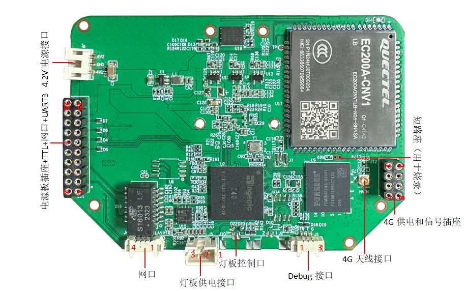
板卡尺寸:90*64mm
CPU参数
1.2.1 CPU
XBurst®2 up to 1.2GHz, Dual Core, Dual-issue, high performance and low power implementation
of MIPS32 ISA R5
MIPS32 ISA R5 plus Ingenic SIMD512 ISA
Dual-issue, superscalar, super pipeline with Simultaneous Multi-Threading(SMT)
Two
hardware threads per physical core
Quad
instruction fetches per cycle
Dual
issue instructions per cycle per thread
32K L1 D cache + 32K L1 I cache, 128~1024K L2 cache
High-performance Floating-point Unit and SIMD Engine: FSE
32x512-
bit register set, 512-bit loads/stores to/from SIMD unit
IEEE-
754 2008 compliant
Programmable Memory Management Unit(MMU)
1st
level mini-TLBs(MTLBs)-8x2 entry instruction TLB, 16x2 entry data TLB
2nd
level TLBs:32x2 entry VTLB, 256x2 entry 4-way set associative FTLB
The XBurst®2 processor system supports little endian only
1.2.2 MCU
600MHz RISC-V coprocessor
32bit, in-order, 5-stage pipeline core
32K L1-cache and 32K L1 D-cache
RV32IM instruction set architecture
1.2.3 AI Engine
Built-in neural network accelerator
Typical Performance: 8TOPS
Support int16/int8/int4/int2 bit width
Shared 1MB memory pool
Magik AI algorithm develop platform available
1.2.4 AI Co-Processing Unit(AIU)
Color conversion
Resize
Hardware matrix operations
1.2.5 Video Processor Unit(VPU)
Support H.264/H.265/JPEG combo Encoder
Real-time H.256/H.264 encoding capabilities:3840x2160@30fps
Support maximum resolution up to 4096x4096
JPEG snapshot at 8 megapixels
1.2.6 Image Signal Processor(ISP)
Support up to 3 sensors
Support MIPI and DVP interface sensor
Support maximum resolution 3840x2160
3A (Auto Exposure/Auto White Balance/Auto Focus) and able to output the statistical
information
Green equalization
Black level correction
Lens Shading Correction
Lens Distortion Correction
Dynamic/Static Defect pixel correction
Demosaic
2D/3D Color Correction
Gamma Correction
Brightness/Contrast/Saturation/Hue Adjustment
Adaptive Dynamic Range Compression
Defog, WDR
Adaptive Local Contrast Enhancement
Sharpen
2D/3D Denoise
Chroma Noise Reduction
3 Independent Image Scale Up/Down Engine
Crop, Mirror and Flip
1.2.7 Display Process Controller(DPU)
MIPI-DSI4 interface
― Display size up to 1920x1080@60Hz
SLCD controller
― Display size up to 640x480@60Hz,24BPP
― Support different size of display panel
RGB controller
― Display size up to 1280x720@60Hz,24BPP
― Supports input format, ARGB8888, ARGB1555, RGB888, RGB565, RGB555, YUV422,
YUV420
― Support 4 modes parallel interface, 24-bit, 18-bit, 16-bit and 8-bit(third times)
― Support frame buffer crop and dither
1.2.8 Video Input and Output
Video Input
– Support 8/10/12 bit RGB Bayer input
– Support DVP, BT1120(serial model)/BT656/BT601
– Support MIPI CSI (lane up to 1.5Gbps, and support one 4-Lane or two 2-Lane sensor)
– Support maximum:3840x2160@30fps
– Support up to 3 sensor inputs (DVP/BT, two CSI 2lane)
Video output
– Support BT656 serial/parallel mode
– Support BT1120 serial/parallel mode
– Support MIPI DSI 4lane
1.2.9 Audio System
Integrated Audio Codec
– 24 bits DAC with 93dB SNR
– 24 bits ADC with 92dB SNR
– Support signal-ended and differential microphone input and line input
– Automatic Level Control (ALC) for smooth audio recording
– Pure logic process: no need for mixed signal layers and less mask cost
– Programmable input and output analog gains
– Digital interpolation and decimation filter integrated
– Sampling rate 8K/12K/16K/24K/32/44.1K/48K/96K
Digital MIC controller
– 16 bits data interface and 20bit precision internal controller
– SNR:90dB, THD:-90dB @ FS -20dB
– Linear high pass filter include. Attenuation: -2.9dB@100Hz, -22dB@27Hz, -36dB@10Hz
– Low power voice trigger when waiting to start talking
– 1/2/3/4 channel digital MIC support
– Support voice data pre-fetch when trigger enable and the data interface disable, but do
not increase the power dissipation
– Sample frequency supported: 8K, 16K
– Support low power mode, user for decrease DMIC sensor and DMIC controller power
dissipation
Standard Audio I2S Interface
– 16,20 and 24 bit audio sample data sizes supported, 16 bits packed sample data is
supported
– DMA transfer mode supported
– Stop serial clock supported
– Support mono PCM data to stereo PCM data expansion on audio play back
– Support endian switch on 16-bits normal audio samples play back
– Internal programmable or internal serial clock and optional system clock supported for
I2S or MSB-Justified format
– Two FIFOs for transmit and receive respectively
– Support different sample rate for transmit and receive
– Support echo cancellation function in the condition of the same sample rate in transmit
and receive
1.2.10 Memory Interface
Support up to size 2GB KGD and DDR2, DDR3, DDR3L
1.2.11 System Functions
Clock generation and power management
– On-chip 12/24/48MHZ oscillator circuit
– One four-chip phase-locked loops (PLL) with programmable multiplier
– CCLK, HHCLK, H2CLK, PCLK, H0CLK, DDR_CLK, VPU_CLK frequency can be
changed separately for software by setting registers
– SSI clock supports 50M clock
– MSC clock supports 100M clock
– Functional-unit clock gating
– Shut down power supply for CPU, ISP, VPU, IPU
Timer and counter unit with PWM output and/or input edge counter
– Provide eight separate channels, six of them have input signal transition edge counter
– 16-bit A counter and 16-bit B counter with auto-reload function every channel
– Support interrupt generation when the A counter underflow
– Three clock sources: RTCLK (real time clock), EXCLK (external clock input), PCLK (APB
Bus clock) selected with 1, 4, 16, 64, 256 and 1024 clock dividing selected
– Every channel has PWM output
OS timer controller
– 64-bit counter and 32-bit compare register
– Support interrupt generation when the counter matches the compare register
– Two clock sources: RTCLK (real time clock), HCLK (system bus clock) selected with 1, 4,
16, 64, 256 and 1024 clock dividing selected
Interrupt controller
– Total 64 interrupt sources
– Each interrupt source can be independently enabled
– Priority mechanism to indicate highest priority interrupt
– All the registers are accessed by CPU
– Unmasked interrupts can wake up the chip in sleep mode
– Another set of source, mask and pending registers to serve for PDMA
Watchdog timer
– Generates WDT reset
– A 16-bit Data register and a 16-bit counter
– Counter clock uses the input clock selected by software
PCLK, EXTAL and RTCLK can be used as the clock for counter
The division ratio of the clock can be set to 1, 4, 16, 64, 256 and 1024 by software
Direct memory access controllers
– Support up to 32 independent DMA channels
– Descriptor or No-Descriptor Transfer mode compatible with previous JZ SoC
– Transfer data units: 1-byte, 2-byte, 4-byte, 16-byte, 32-byte, 64-byte, 128-byte
– Transfer number of data unit: 1 ~ 224 - 1
– Independent source and destination port width: 8-bit, 16-bit, 32-bit
– Fixed three priorities of channel groups: 0~3, highest; 4~11: mid; 12~31: lowest
– An extra INTC IRQ can be bound to one programmable DMA channel
SAR A/D Interface
– 4 single-ended input channels and 4 Standard I/O cell multiplexed
– 12-bit resolution, up to 2MS/s sampling rate
– DNL<1LSB,INL<2LSB
– Max Frequency: 24MHz
– Current consumption:2.5mA@2MS/s
OTP Slave Interface
– Total 2048 bits. and used as 1024 bits for safe
Power On Reset(POR)
– Provides reliable reset function for general applications
– Monitor 1.8V supply for IO and 0.9V for core
– Typical 1.35V threshold for 1.8V supply
– Typical 0.6V threshold for 0.9V supply
1.2.12 Peripherals
General-Purpose I/O ports
– Input/output/function port configurable
– Low/high, rising/falling edge triggering. Every interrupt source can be masked
independent
– four interrupts, each interrupt corresponds to the group, to INTC
Four I2C Controller(SMB0, SMB1, SMB2, SMB3)
– Two-wire I2C serial interface – consists of a serial data line (SDA) and a serial clock
(SCL)
– Three speeds mode
Standard mode (100 Kb/s)
Fast mode (400 Kb/s)
High speed mode(3.4Mb/s)
– Programmable SCL generator
– Master or slave I2C operation
– 7-bit addressing/10-bit addressing
– The number of devices that you can connect to the same I2C-bus is limited only by the
maximum bus capacitance of 400pF
One High Speed Synchronous serial interfaces (SFC)
– 3 protocols support: National’s Microwire, TI’s SSP, and Motorola’s SPI
– transmit-only or receive-only operation
– MSB first for command and data transfer, and LSB first for address transfer
– 64 entries x 32 bits wide data FIFO
– one device select
– Configurable sampling point for reception
– Configurable timing parameters: tSLCH, tCHSH and tSHSL
– Configurable flash address wide are supported
– transfer formats: Standard SPI only
– two data transfer mode: slave mode and DMA mode
– Configurable 6 phases for software flow
Normal Speed Synchronous serial interfaces (SSI0, SSI1)
– 3 protocols support: National’s Microwire, TI’s SSP, and Motorola’s SPI
– Full-duplex or transmit-only or receive-only operation
– Programmable transfer order: MSB first or LSB first
– 128 entries deep x 32 bits wide transmit and receive data FIFOs
– Configurable normal transfer mode or Interval transfer mode
– Programmable clock phase and polarity for Motorola’s SSI format
– Back-to-back character transmission/reception mode
– Loop back mode for testing
Four UARTs (UART0, UART1, UART2,UART3)
– Full-duplex operation
– 5-, 6-, 7- or 8-bit characters with optional no parity or even or odd parity and with 1, 1½,
or 2 stop bits
– 64x8 bit transmit FIFO and 64x11bit receive FIFO
– Independently controlled transmit, receive (data ready or timeout), line status interrupts
– Internal diagnostic capability Loopback control and break, parity, overrun and
framing-error is provided
– Separate DMA requests for transmit and receive data services in FIFO mode
– Supports modem flow control by software or hardware
– Slow infrared asynchronous interface that conforms to IrDA specification
Two MMC/SD/SDIO controllers (MSC0, MSC1)
– All support eMMC 5.1(command queueing Engine)
– Support SD Specification 3.0
– Support SD I/O Specification 1.0 with 1 command channel and 4 data channels
– Consumer Electronics Advanced Transport Architecture (CE-ATA – version 1.1)
– Maximum data rate is 104MBps
– Both support MMC data width 1bit, 4bit
– Single or multi block access to the card including erase operation
– The maximum block length is 4096bytes
USB 2.0 OTG interface
– Complies with the USB 2.0 standard for high-speed (480 Mbps) functions and with the
On-The-Go supplement to the USB 2.0 specification
– Operates either as the function controller of a high- /full-speed USB peripheral or as the
host/peripheral in point-to-point or multi-point communications with other USB functions
– Supports Session Request Protocol (SRP) and Host Negotiation Protocol (HNP)
– UTMI+ Level 3 Transceiver Interface
– Soft connect/disconnect
– 16 Endpoints
– Dedicate FIFO
– Supports control, interrupt, ISO and bulk transfer
Ethernet Media Access controller
– 10/100 Mbps operation
– Supports MII and RMII PHY interfaces
– Support IEEE 1588-2002
Digital True Random Number Generator(DTRNG)
– Pure digital logic circuits
– True random number
– Interrupt mode and no interrupt mode
1.2.13 Bootrom
22kB Boot ROM memory
接口电路
4.2V电源接口
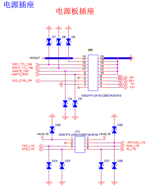
电源板插座+TTL+网口+UART3+4G供电和信号接口
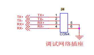
网口
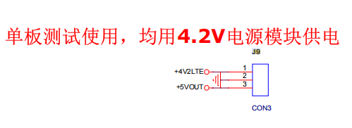
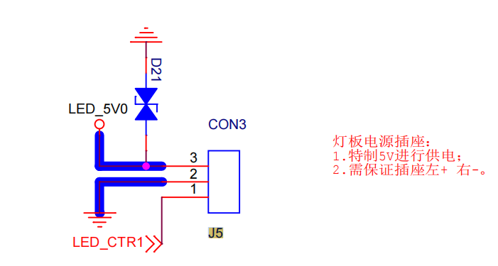
灯板供电接口
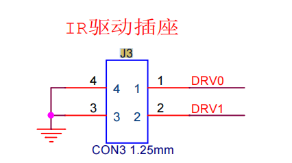
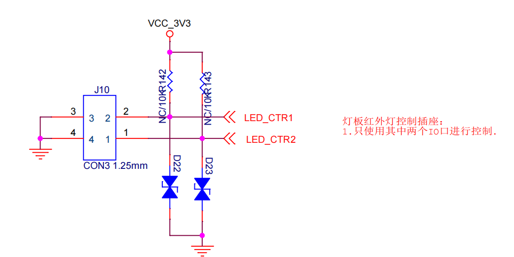
灯板控制接口
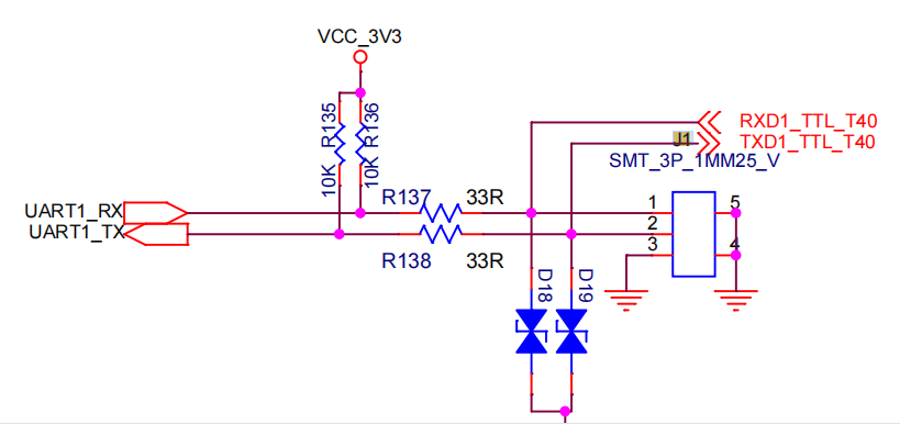
Debug口
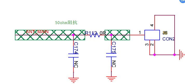
4G天线接口
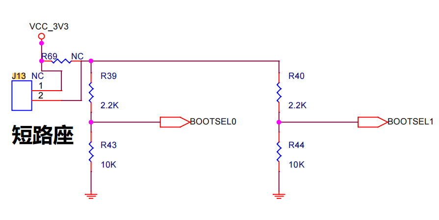
短路座(用于烧录)
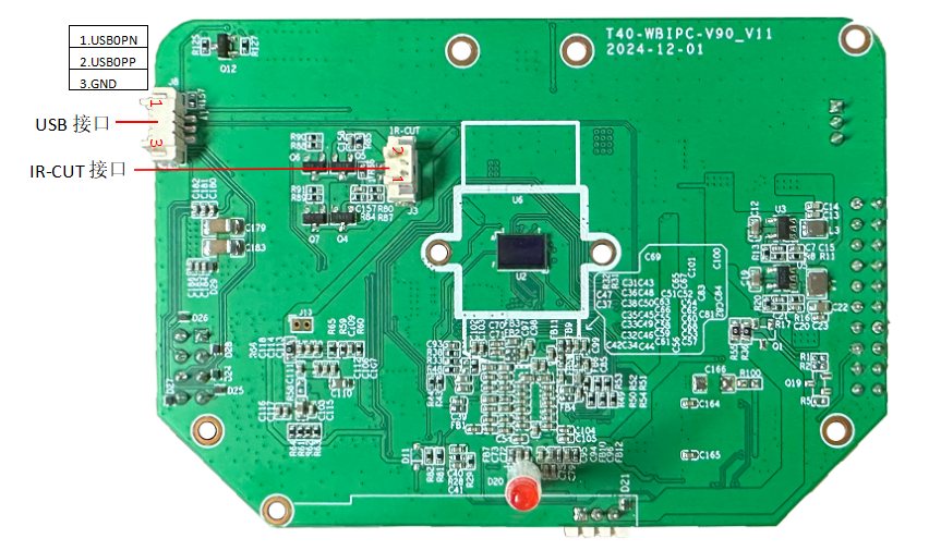
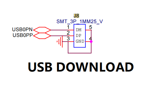
USB接口
IR-CUT接口